Closed loop backdrilling system

a backdrilling system and closed loop technology, applied in emergency protective circuit arrangements, waveguides, etc., can solve the problem of changing the amount of stub portion which needs to be removed, disconnecting the signal layer, and uneven thickness of the various layers of the multi-layer circuit board

Inactive Publication Date: 2006-08-29
VIASYST
View PDF29 Cites 48 Cited by
  • Summary
  • Abstract
  • Description
  • Claims
  • Application Information

AI Technical Summary

Problems solved by technology

However, in practice the thicknesses of the various layers in the multilayer circuit boards are not uniform, and the depths of the signal layers within the multilayer circuit boards vary, which often changes the amount of the stub portion which needs to be removed.
Drilling too deeply will disconnect the signal layer from the plated hole, or leave an unreliable connection; not drilling deep enough decreases the signal to noise ratio.

Method used


Image

  • Closed loop backdrilling system
  • Closed loop backdrilling system
  • Closed loop backdrilling system

Examples


Embodiment Construction

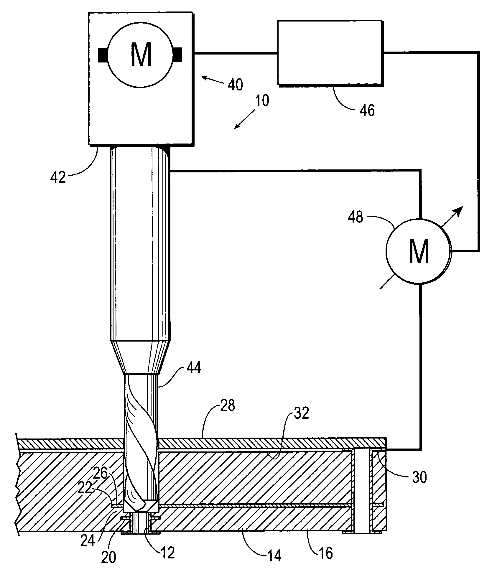
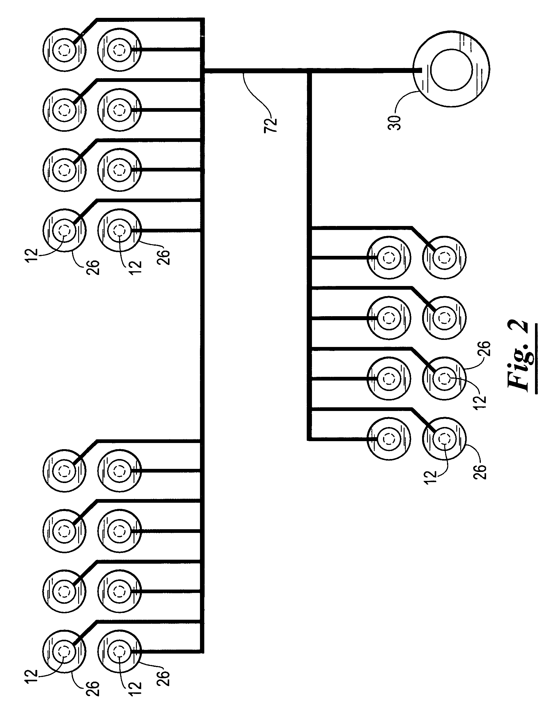
[0018]Referring now to the drawings and in particular to FIG. 1, shown therein and designated by a reference numeral 10 is a closed loop backdrilling system constructed in accordance with the present invention. The closed loop backdrilling system 10 is used for depth drilling an already plated hole 12 formed in a workpiece 14 using electrical feedback from the workpiece 14 when a certain or predetermined depth is reached. The feedback during the drilling process makes it possible to yield much higher accuracy independent of the depth of a particular layer within the workpiece 14. In one preferred embodiment, the workpiece 14 is a multilayer printed circuit board 16. Although the workpiece 14 will be described herein as the multilayer circuit board 16, it should be understood that the workpiece 14 can be any apparatus, or device where it is desirable to drill to a certain or predetermined depth within the apparatus or device.

[0019]The multilayer circuit board 16 is provided with at l...


PUM

PropertyMeasurementUnit
diameteraaaaaaaaaa
non-conductiveaaaaaaaaaa
areaaaaaaaaaaa

Abstract

A multilayer circuit board is provided with at least one signal layer, at least one feedback layer, and at least one dielectric layer positioned between the signal layer and the feedback layer. The signal layer is connected to at least one plated hole. The feedback layer has a contact pad, which is positioned adjacent to the plated hole, but is electrically isolated from the plated hole. The contact pad is connected to a measurement unit. The dielectric layer is positioned between the signal layer and the contact pad of the feedback layer. A portion of the plated hole forms a stub portion, which extends a distance away from the signal layer and typically extends a distance away from the contact pad of the feedback layer. To remove the stub portion, a hole is bored or routed into the multilayer circuit board until electrical feedback is received by the measurement unit upon contact of a portion of the boring device with the contact pad. Upon receipt of the electrical feedback by the measurement unit, the boring device is retracted from the hole, and the hole formed by the boring device is filled with an epoxy, or other filler material.

Description

CROSS-REFERENCE TO RELATED APPLICATIONS[0001]The present patent application claims priority to the provisional patent application identified by U.S. Ser. No. 60 / 504,399, filed on Sep. 19, 2003, the entire content of which is hereby incorporated herein by reference.BACKGROUND OF THE INVENTION[0002]Multilayer circuit boards and / or wiring boards are well known in the art. The multilayer circuit boards are formed with a number of signal layers (conductive layers) which are arranged in a predetermined pattern. The signal layers are insulated from each other by dielectric layers. Thus, the multilayer circuit board is formed from interleaved (e.g., alternating) signal layers and dielectric layers.[0003]Plated holes or “vias” are formed through the multilayer circuit board to connect one signal layer to another signal layer. The plated holes typically extend from one main side of the multilayer circuit board to an opposite side of the multilayer circuit board. In some instances, the plated ...

Claims


Application Information

Patent Timeline
Patent Type & Authority Patents(United States)
IPC IPC(8): B23P6/00H05K1/16H02H1/04H05K1/02H05K1/11H05K3/00H05K3/42
CPCH05K3/0047H05K3/429H05K1/0237Y10T408/175H05K2201/09845H05K2203/0207H05K2203/0242H05K2203/175Y10T29/49718Y10T29/49726Y10T408/173Y10T29/49165Y10T29/49126Y10T29/49117Y10T408/03H05K1/0268
Inventor TOURNE, JOSEPH A. A. M.LEBENS, PATRICK P. P.
Owner VIASYST
Why Eureka
Try Eureka