Multi-chip configuration to connect flip-chips to flip-chips

a multi-chip configuration and flip-chip technology, applied in the field of semiconductor devices, can solve the problems of reducing the performance of the package, affecting the integration of devices, and many prior stacking techniques do not provide direct connections between stacking dice, so as to improve heat dissipation, reduce signal propagation delays, and improve device integration

Active Publication Date: 2006-08-29
XILINX INC
View PDF5 Cites 86 Cited by
  • Summary
  • Abstract
  • Description
  • Claims
  • Application Information

AI Technical Summary

Benefits of technology

[0007]A multi-chip package is disclosed that includes a carrier configured to house overlying layers of staggered IC dice that can be flip-chip mounted to each other in a cascade configuration to minimize signal propagation delays between the dice. For some embodiments, the dice in one layer of the package can also be flip-chip mounted to corresponding pads on the carrier. By staggering the dice in one layer with respect to the dice in another layer so that the dice are not stacked directly on top of one another, heat dissipation can be improved over prior vertical stacking techniques. Further, because present embodiments include multiple layers of dice, device integration is greater than prior packages that have only one layer of dice.

Problems solved by technology

Although such multi-chip packages allow multiple dice to be enclosed in a single package, propagation delays of signals transmitted between the dice via the substrate's interconnect circuitry can reduce performance of the package.
In addition, these long signal lines are susceptible to noise that can further degrade performance.
However, many prior stacking techniques do not provide direct connections between the stacked dice, but rather rely upon the carrier's interconnect circuitry to provide such connections.
Further, because the dice are stacked on top of one another, the amount of power being dissipated within the same area (e.g., the area of one chip) significantly increases, and can cause undesirable and potentially damaging local heating or “hot spots” on the dice.

Method used


Image

  • Multi-chip configuration to connect flip-chips to flip-chips
  • Multi-chip configuration to connect flip-chips to flip-chips
  • Multi-chip configuration to connect flip-chips to flip-chips

Examples


Embodiment Construction

[0020]The present invention is applicable to a variety of integrated circuits and systems. In the following description, for purposes of explanation, specific nomenclature is set forth to provide a thorough understanding of the present invention. However, it will be apparent to one skilled in the art that these specific details may not be required to practice the present invention. In other instances, well-known circuits and devices are shown in block diagram form to avoid obscuring the present invention. Accordingly, the present invention is not to be construed as limited to specific examples described herein but rather includes within its scope all embodiments defined by the appended claims.

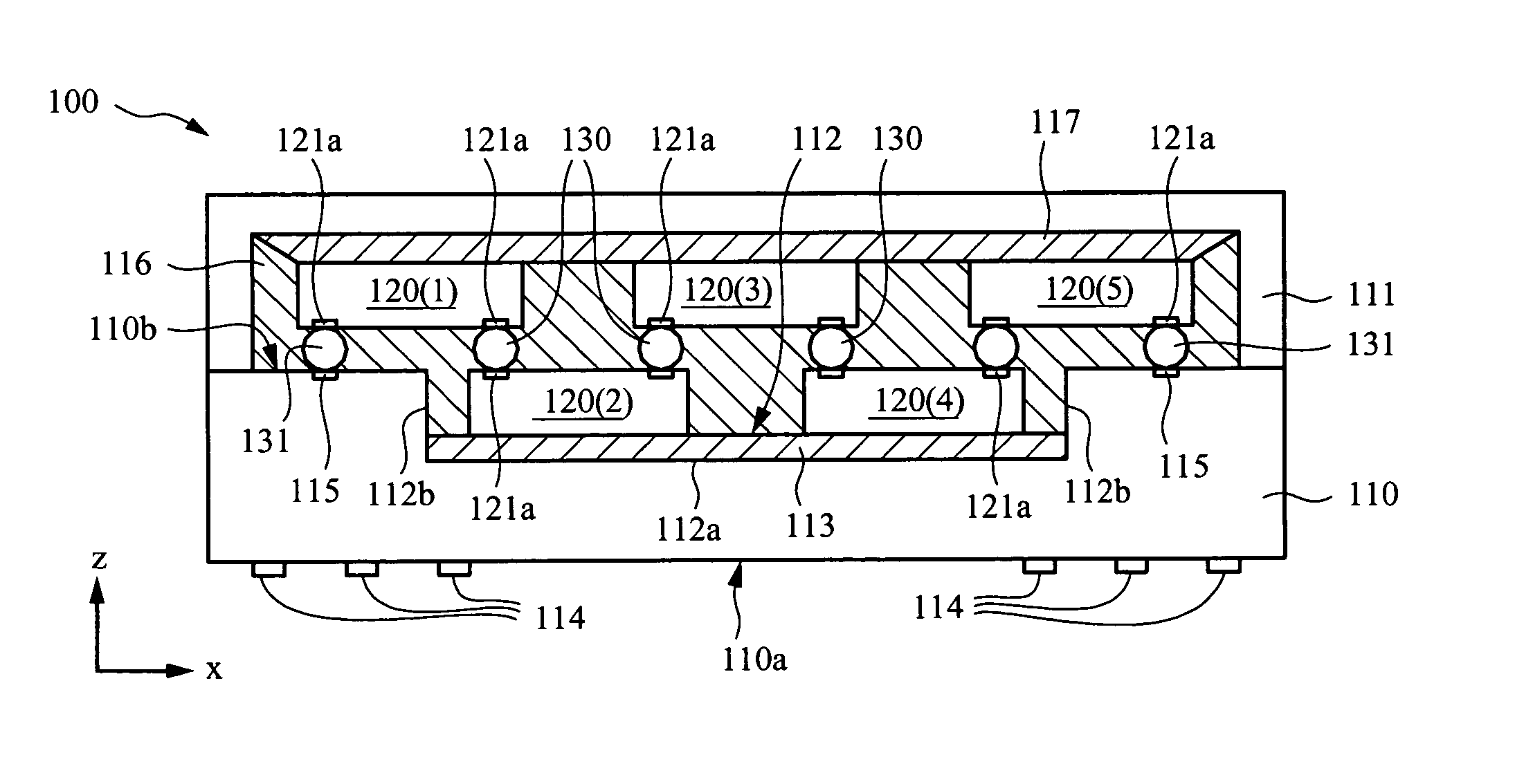
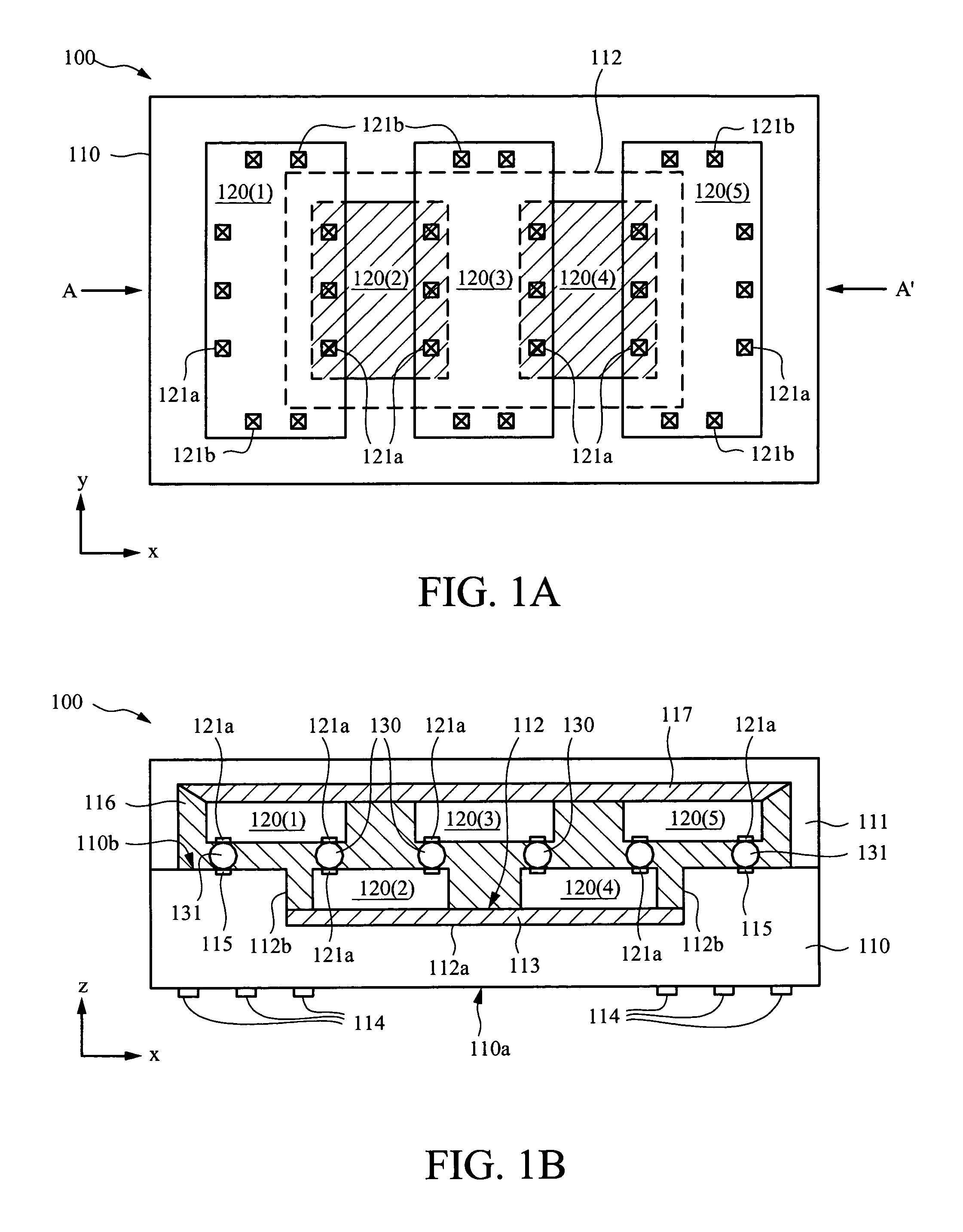
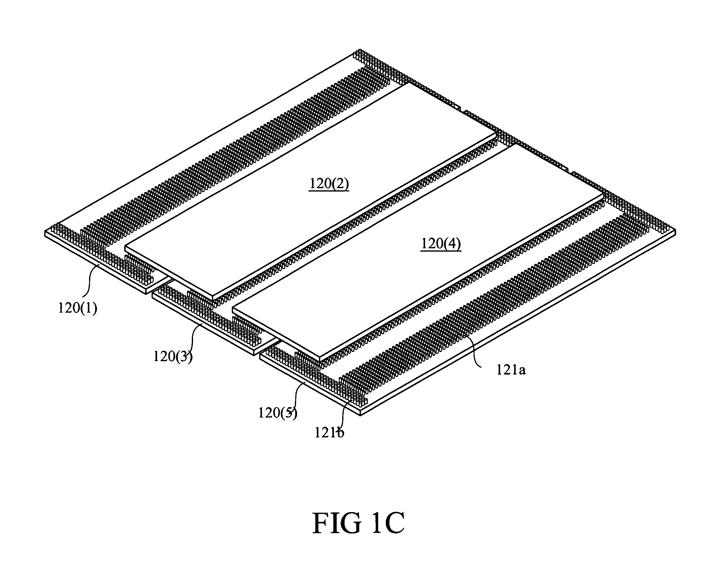
[0021]FIGS. 1A–1C show a multi-chip package 100 in accordance with one embodiment of the present invention. (Note that portions of multi-chip package 100 shown in FIG. 1C are shown upside down for clarity.) Package 100 includes a substrate or carrier 110 and a lid 111 adapted to house any numbe...


PUM


Abstract

A semiconductor structure includes a carrier having a cavity formed in a top portion thereof, and a plurality of conductive contacts formed on a top surface of the carrier and positioned around the periphery of the cavity. A number of first coplanar dice are back-side mounted to a top surface of the cavity, and a number of second coplanar dice are flip-chip mounted to the first dice, wherein each of the first dice is electrically connected to two corresponding adjacent second dice to connect the dice in a cascade configuration. For some embodiments, selected dice are flip-chip mounted to the carrier. For other embodiments, selected dice are wire-bond connected to the carrier.

Description

FIELD OF INVENTION[0001]The present invention relates generally to semiconductor devices, and more specifically to semiconductor packages containing multiple integrated circuits.DESCRIPTION OF RELATED ART[0002]Typically, a plurality of integrated circuits (ICs) is formed on a semiconductor (e.g., silicon) wafer, which is then cut or “diced” to separate individual ICs from one another. The resulting bare IC dice (e.g., chips) are then packaged to protect them from external conditions. An IC package typically includes an IC die mounted on a substrate and encapsulated with a protective material. Conductive pads formed on the die are electrically connected to corresponding contacts formed on a first surface of the substrate. External leads formed on a second surface of the substrate and electrically connected to the pads on the first surface via the substrate's interconnect circuitry provide electrical connections to external systems (e.g., to other packaged dice).[0003]A variety of die...

Claims


Application Information

Patent Timeline
Patent Type & Authority Patents(United States)
IPC IPC(8): H01L23/48H01L23/02
CPCH01L23/13H01L23/24H01L25/0652H01L2224/16H01L2224/731H01L2224/73253H01L2924/16152H01L2924/01078H01L2924/15153H01L2924/15165H01L24/73H01L2224/0554H01L2224/0557H01L2224/05571H01L2224/05573H01L2224/06135H01L2224/16145H01L2224/16225H01L2224/48091H01L2224/48227H01L2224/73207H01L2224/73265H01L2924/00014H01L2924/14H01L2924/15156H01L2224/32225H01L2924/00012H01L2924/00H01L2224/05599H01L2224/0555H01L2224/0556
Inventor HOANG, LAN H.WU, PAUL YING-FUNG
Owner XILINX INC
Why Eureka
Try Eureka