Semiconductor display device and method of driving semiconductor display device

Inactive Publication Date: 2006-08-29
SEMICON ENERGY LAB CO LTD
View PDF24 Cites 20 Cited by
  • Summary
  • Abstract
  • Description
  • Claims
  • Application Information

AI Technical Summary

Benefits of technology

[0049]In view of the above, an object of the present invention is to provide a method of driving a semiconductor display device which is capable of displaying a clear, high definitio

Problems solved by technology

In other words, pixels to which display signals having the same polarity are inputted are changed irregularly in a cer

Method used


Image

  • Semiconductor display device and method of driving semiconductor display device
  • Semiconductor display device and method of driving semiconductor display device
  • Semiconductor display device and method of driving semiconductor display device

Examples


embodiment mode 1

[Embodiment Mode 1]

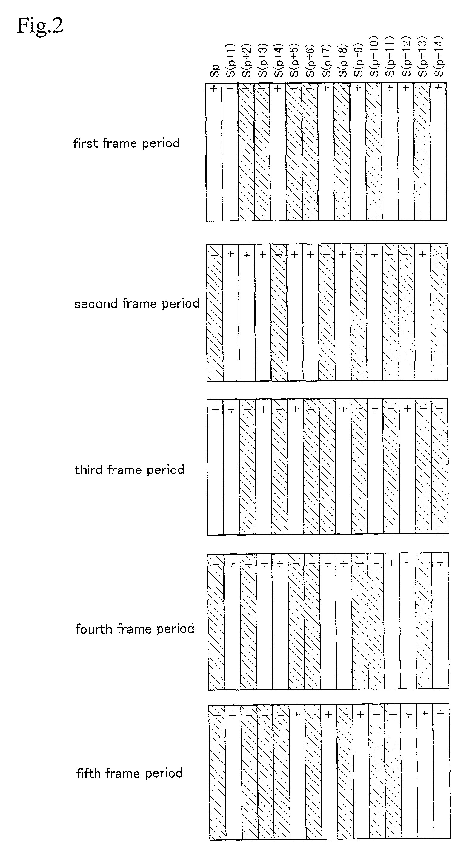
[0203]A polarity pattern of each pixel in an alternating current drive of the present invention is shown in FIG. 2. Note that, in order to simplify the explanation, the polarity pattern of only pixels connected to 15 arbitrary adjacent source signal lines Sp, S(p+1), S(p+2), . . . , S(p+14) among the source signal lines S1 to Sx, is shown. Further, the pixels connected to each source signal line are not separated but are shown as one rectangle in Embodiment mode 1. Further, FIG. 3 is a diagram showing the electric potential of display signals inputted to each source line in the alternating current driving of Embodiment mode 1, shown in FIG. 2, in a case in which an active matrix liquid crystal display device performing white display provided it is normally black, and performing black display provided it is normally white.

[0204]The polarities of the display signals inputted to the pixels connected to the source signal lines Sp, S(p+1), S(p+2), . . . , S(p+14) becom...

embodiment mode 2

[Embodiment Mode 2]

[0213]An example of a driving method of the present invention, which is different from that shown in Embodiment mode 1, is explained in Embodiment mode 2.

[0214]A polarity pattern of each pixel in an alternating current drive of the present invention is shown in FIG. 4. Note that, in order to simplify the explanation, the polarity pattern of only pixels connected to 15 arbitrary and adjacent source signal lines Sp, S(p+1), S(p+2), . . . , S(p+14) among the source signal lines S1 to Sx, is shown. Further, the pixels connected to each source signal line are not separated but are shown as one rectangle in Embodiment mode 2.

[0215]The polarities of display signals inputted to the pixels connected to the source signal lines Sp, S(p+1), S(p+2), . . . , S(p+14) become positive, negative, positive, positive, negative, positive, negative, positive, negative, negative, positive, negative, negative, positive, and positive, respectively, in a first frame period. Namely, the dis...

embodiment mode 3

[Embodiment Mode 3]

[0225]An example of a driving method of the present invention, which is different from that shown in Embodiment modes 1 and 2, is explained in Embodiment mode 3.

[0226]A polarity pattern of each pixel in an alternating current drive of the present invention is shown in FIG. 5. Note that, in order to simplify the explanation, the polarity pattern of only pixels connected to 15 arbitrary and adjacent source signal lines Sp, S(p+1), S(p+2), . . . , S(p+14) among the source signal lines S1 to Sx, is shown. Further, the pixels connected to each source signal line are not separated but are shown as one rectangle in Embodiment mode 3.

[0227]The polarities of display signals inputted to the pixels connected to the source signal lines Sp, S(p+1), S(p+2), . . . , S(p+14) in a first frame period become positive, negative, positive, negative, positive, negative, positive, negative, positive, negative, positive, negative, positive, negative, and positive, respectively, inverted ...


PUM


Abstract

A semiconductor display device with which flicker, vertical striping, and horizontal striping are not easily seen, and a method of driving the semiconductor display device, are provided. Display signals inputted to a plurality of pixel electrodes have a positive or negative polarity based on the electric potential of an opposing electrode, and pixel electrodes to which display signals having a positive polarity are inputted, and pixel electrodes to which display signals having a negative polarity are inputted, differ for each frame period with the method of driving the semiconductor display device.

Description

BACKGROUND OF THE INVENTION[0001]1. Field of the Invention[0002]The present invention relates to a very suitable driving method for a semiconductor display device using a display medium such as liquid crystals, and to a semiconductor display device which performs display using the driving method. In particular, the present invention relates to a method of driving an active matrix liquid crystal display device, and to an active matrix liquid crystal display device which performs display using the driving method.[0003]2. Description of the Related Art[0004]Techniques of manufacturing an element formed using a semiconductor thin film on an insulating substrate, a thin film transistor (TFT) for example, have been rapidly developing in recent years. The reason for the demand is that the demand for semiconductor display devices (typically active matrix liquid crystal display devices) has risen.[0005]Active matrix liquid crystal display devices display an image by controlling electric char...

Claims


Application Information

Patent Timeline
IPC IPC(8): G09G3/36H01L21/77H01L21/84H01L27/12
CPCG09G3/3614G09G3/3648G09G3/3666H01L27/1214G09G2320/0247H01L27/12G09G2320/0219
Inventor ONOYA, SHIGERU
Owner SEMICON ENERGY LAB CO LTD
Why Eureka
Try Eureka