

Semiconductor device and method of manufacturing semiconductor device
- Summary
- Abstract
- Description
- Claims
- Application Information
AI Technical Summary
Benefits of technology
Problems solved by technology
Method used
Image

Examples
Embodiment Construction
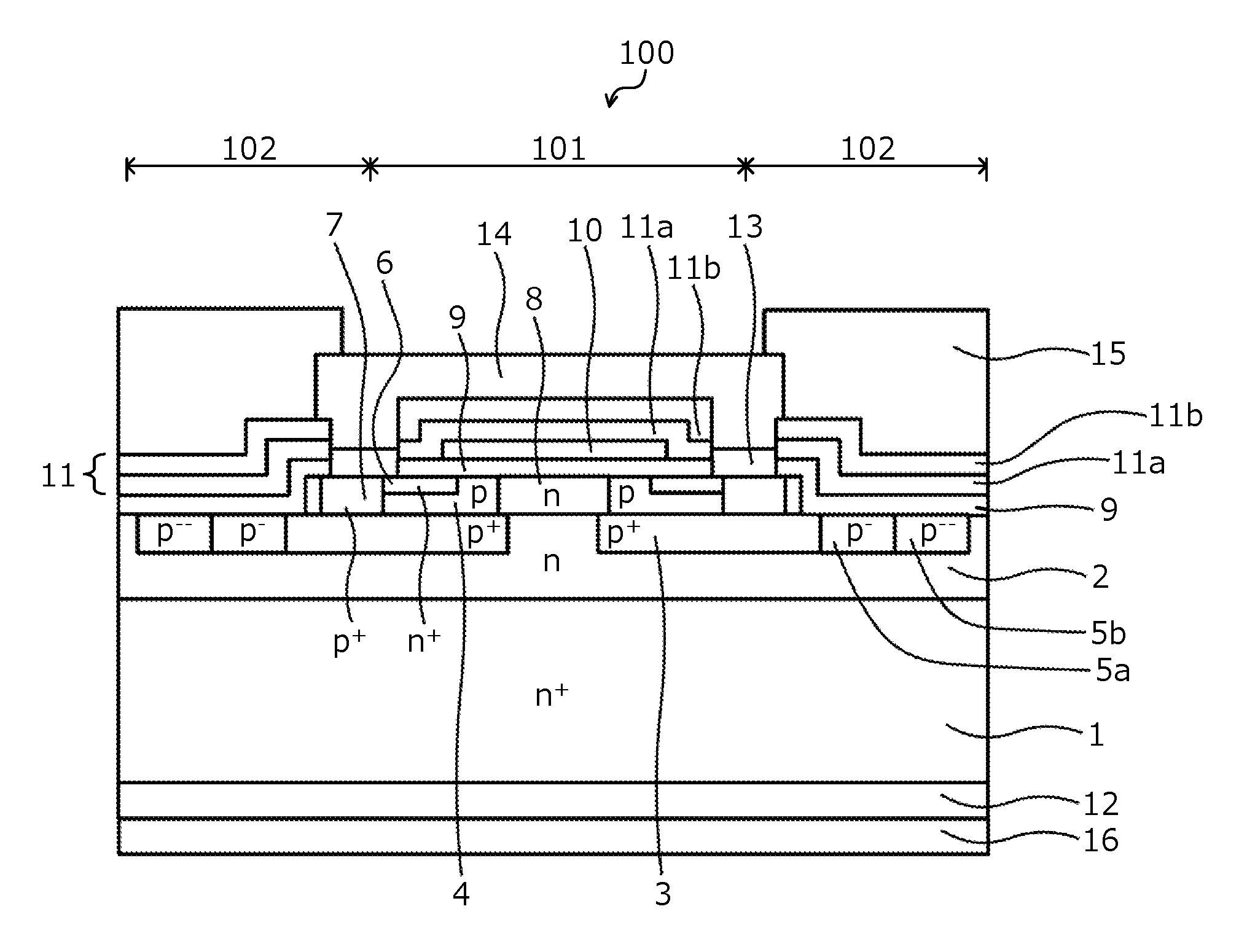
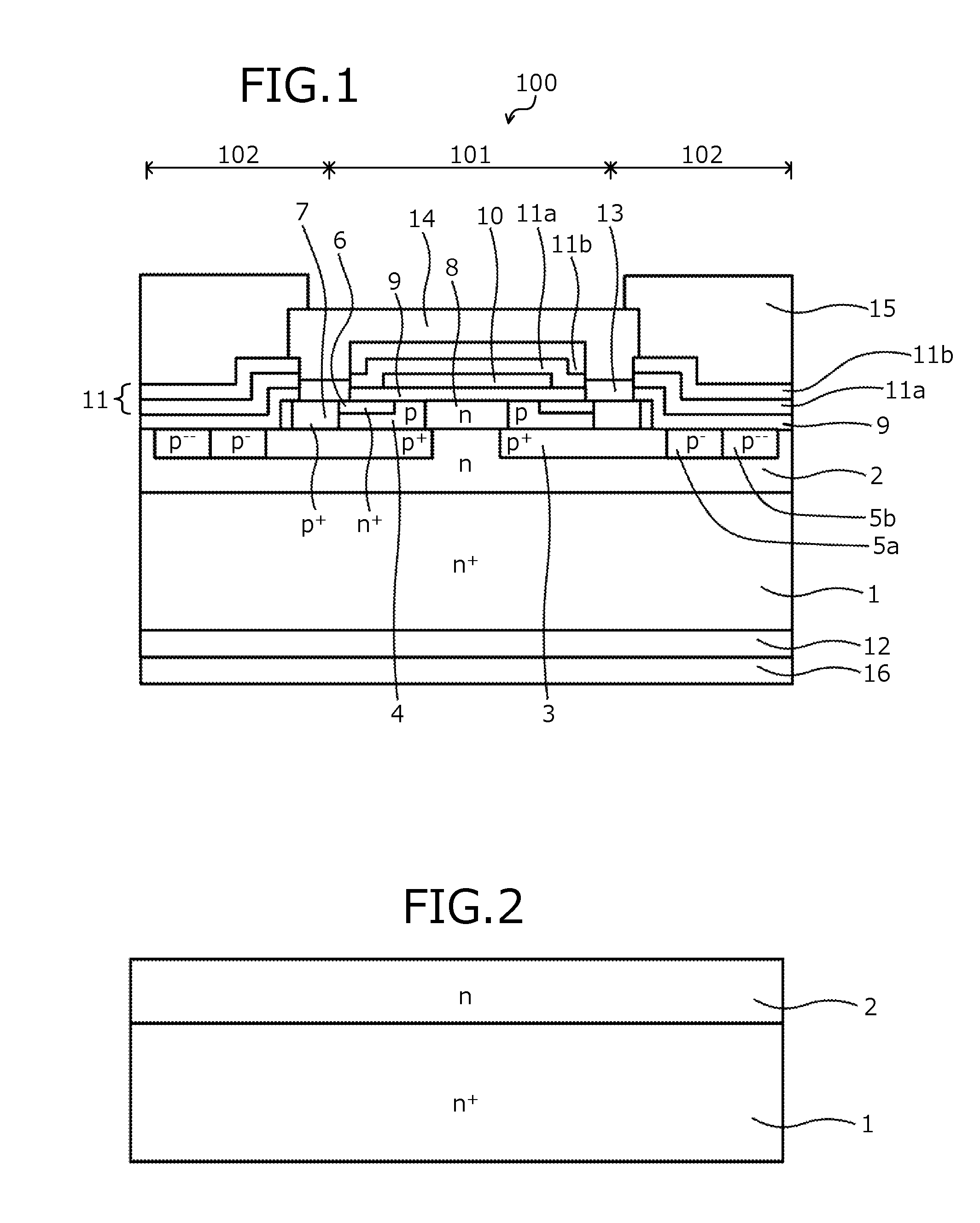
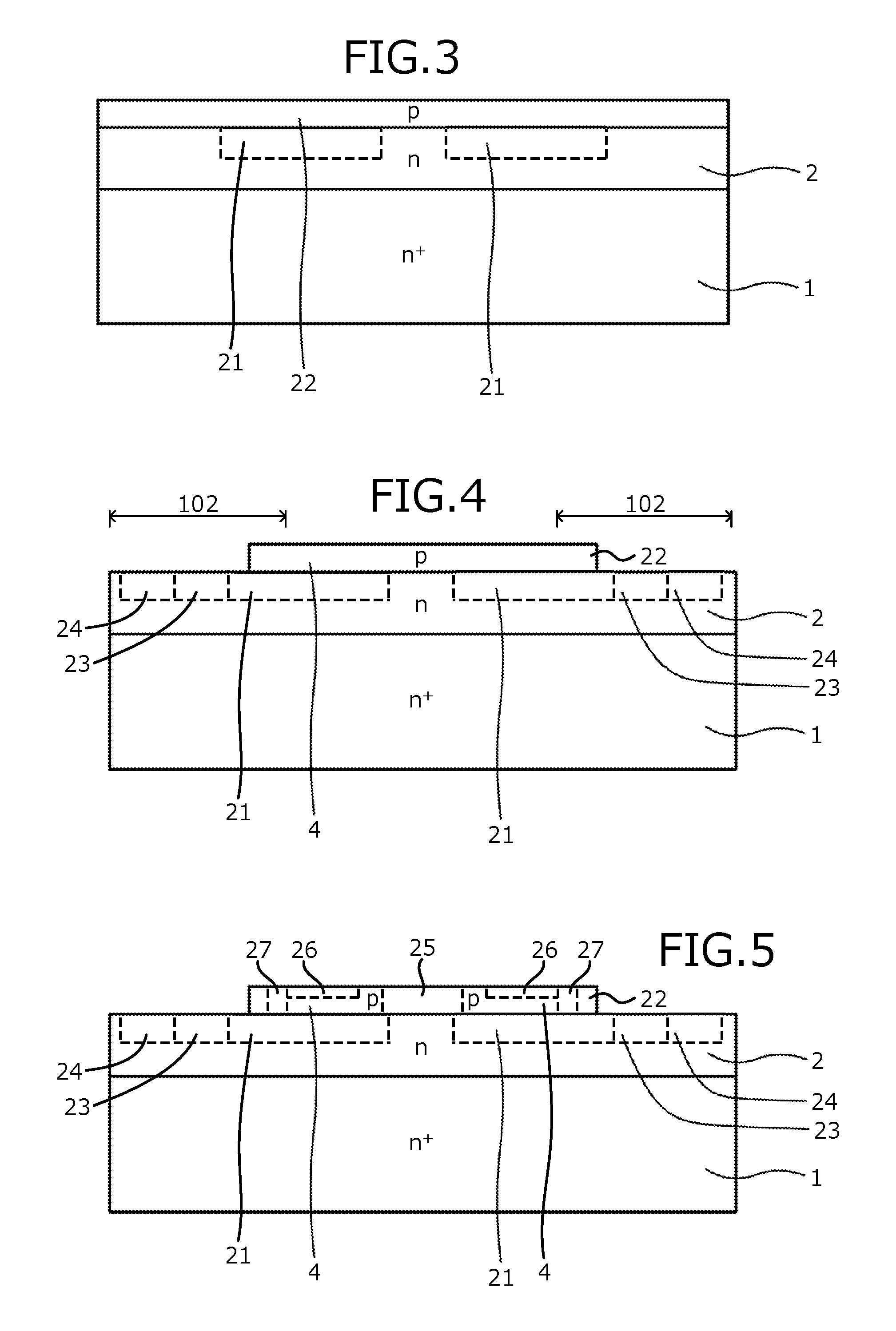
[0028]Embodiments of a semiconductor device and a method of manufacturing a semiconductor device according to the present invention will be described in detail with reference to the accompanying drawings. In the present description and accompanying drawings, layers and regions prefixed with n or p mean that majority carriers are electrons or holes. Additionally, + or − appended to n or p means that the impurity concentration is higher or lower, respectively, than layers and regions without + or −. In the description of the embodiments below and the accompanying drawings, identical constituent elements will be given the same reference numerals and will not be repeatedly described. Further, −− appended to p means that the impurity concentration is lower than that of p-type layers and regions appended with −. Further, in the present description, when Miller indices are described, “−” means a bar added to an index immediately after the “−”, and a negative index is expressed by prefixing...
PUM
 Abstract
Description
Claims
Application Information