Static random access memory and pseudo-static noise margin measuring method

a random access memory and noise margin technology, applied in static storage, information storage, digital storage, etc., can solve the problems of long measurement time, data destruction is harder to occur, and the inability to measure snm in memory cells on chips as products,

Inactive Publication Date: 2006-08-29
KK TOSHIBA
View PDF4 Cites 29 Cited by
  • Summary
  • Abstract
  • Description
  • Claims
  • Application Information

AI Technical Summary

Problems solved by technology

In general, the larger the SNM, the harder it is for data destruction to occur because of power-source voltage noise in a chip.
The above method, however, enables only the measurement of SNM in the measurement memory cells, but cannot measure SNM in memory cells on chips as products.
Further, since an actual measurement is made in a state that pins are attached to respective pads in each measurement cell, a very long measurement time is required, and the amount of data obtained is limited.

Method used


Image

  • Static random access memory and pseudo-static noise margin measuring method
  • Static random access memory and pseudo-static noise margin measuring method
  • Static random access memory and pseudo-static noise margin measuring method

Examples


first embodiment

(First Embodiment)

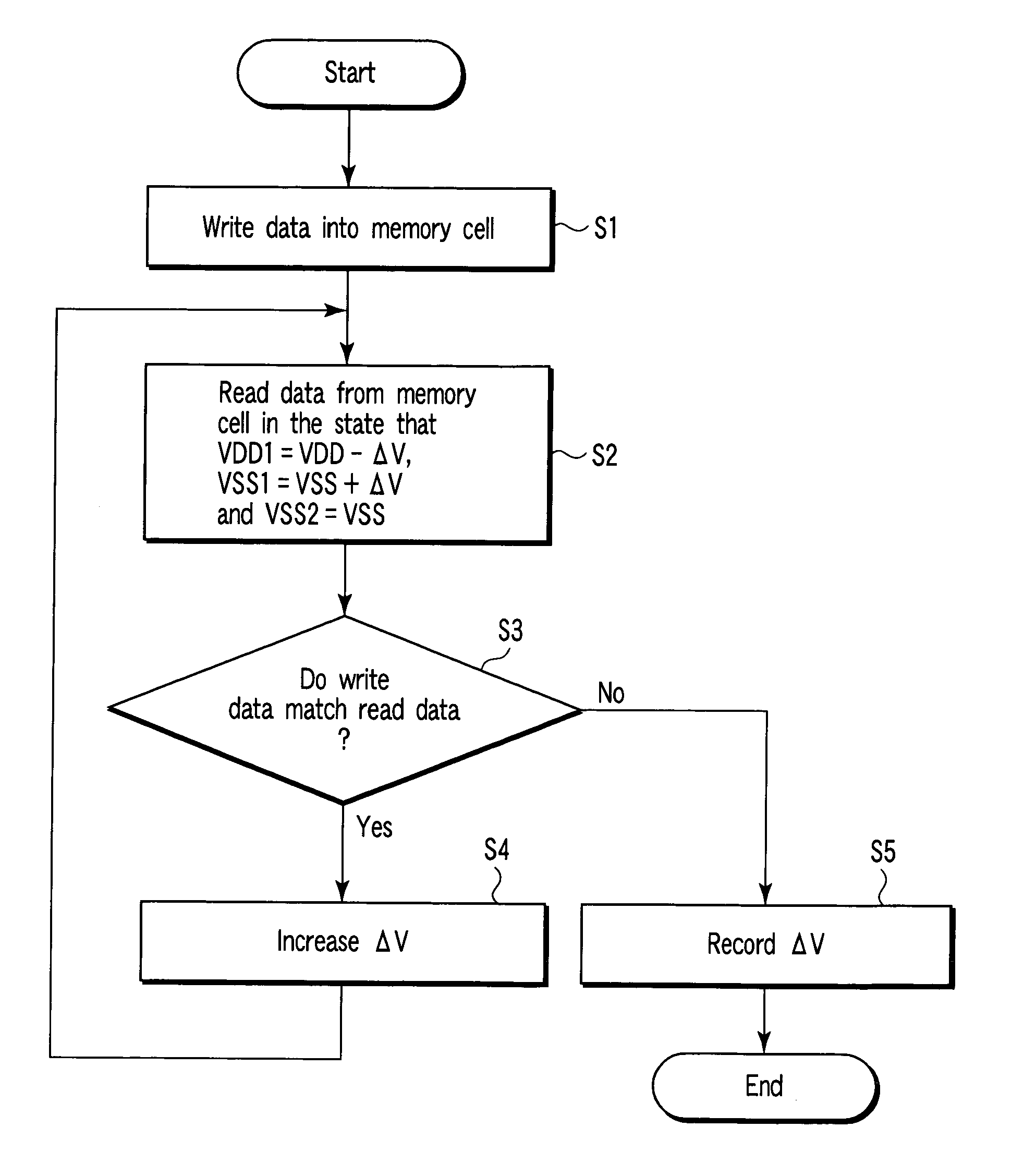
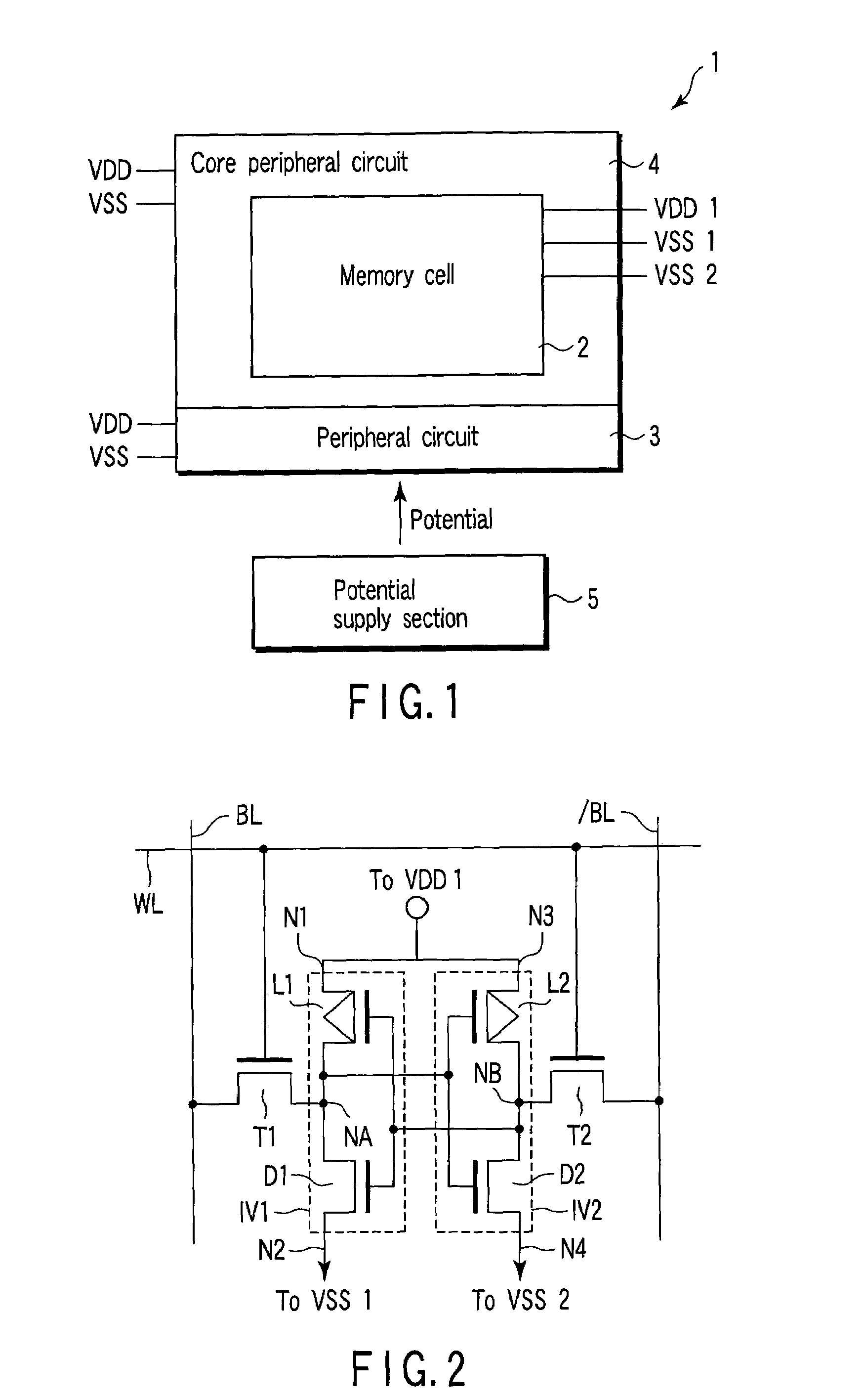
[0023]FIG. 1 is a diagram illustrating a main section of a static random access memory 1 according to a first embodiment of the present invention. As shown in FIG. 1, the static random access memory 1 includes a memory cell array 2, a peripheral circuit 3, and a core periphery circuit 4. The memory cell array 2 has a constitution such that a plurality of memory cells, mentioned later, are provided. The peripheral circuit 3 has a data input / output circuit that gives and receives data to / from an outside, a command / address input circuit that supplies a command and an address to a memory, and a control circuit such as a decoder circuit. The core peripheral circuit 4 has a row decoder, a column decoder, a sense amplifier, and the like.

[0024]The memory cell array 2, the peripheral circuit 3, and the core peripheral circuit 4 are provided with an independent potential supply end. That is to say, the memory cell array 2 is provided with a potential supply end VDD1 for appl...

second embodiment

(Second Embodiment)

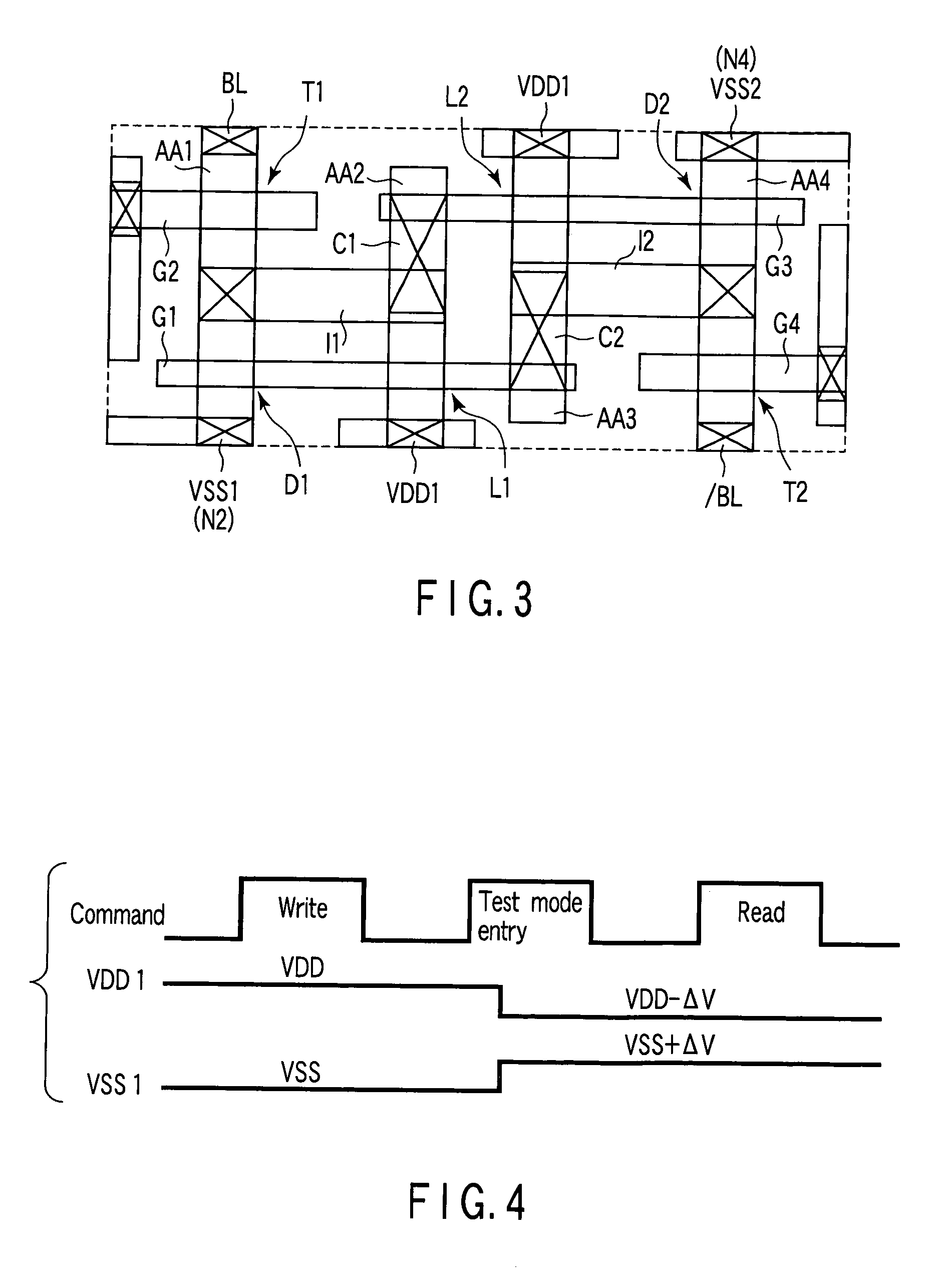
[0046]In the first embodiment, SNM is measured in a state that a uniform potential is applied to the nodes N1 and N3 for applying a high potential to the inverters IV1 and IV2. In contrast, in the second embodiment, different potentials are applied to the nodes N1 and N3, respectively. FIG. 7 is a diagram illustrating a main section of the static random access memory 11 according to a second embodiment of the present invention. FIG. 8 illustrates a state that the memory cell according to the second embodiment, and a state of the potential of the main section in the SNM measuring method according to the second embodiment. As shown in FIGS. 7 and 8, the memory cell 12 has a potential supply end VDD2 for applying a power-source potential in addition to the constitution in FIG. 1. The potential supply end VDD1 is electrically connected to the inverter IV1, and the potential supply end VDD2 is electrically connected to the inverter IV2.

[0047]The SNM measuring method is...


PUM


Abstract

A first inverter includes a first load element and a first transistor, which are connected between first and second terminals in series, a first input terminal and a first output terminal. A second inverter includes a second load element and a second transistor, which are connected between third and fourth terminals in series, a second input terminal and a second output terminal. A first transfer transistor selectively and electrically connects the first output terminal and a first bit line. A second transfer transistor selectively and electrically connects the second output terminal and a second bit line. When data are read from the memory cell which comprises the first and second inverters and the first and second transfer transistors, a first potential is applied to the second terminal and a second potential different from the first potential is applied to the fourth terminal.

Description

CROSS-REFERENCE TO RELATED APPLICATIONS[0001]This application is based upon and claims the benefit of priority from prior Japanese Patent Application No. 2004-322497, filed Nov. 5, 2004, the entire contents of which are incorporated herein by reference.BACKGROUND OF THE INVENTION[0002]1. Field of the Invention[0003]The present invention relates to a static random access memory (SRAM), and for example, a static noise margin (SNM) of a memory cell.[0004]2. Description of the Related Art[0005]The memory cells of an SRAM typically have first and second inverters whose inputs and outputs are connected to each other, and first and second transfer transistors that connect the output ends of the first and second inverters to a bit line pair. The first and second inverters include a load transistor and a driver transistor. Gates of the first and second transfer transistors are connected to a word line WL.[0006]Conventionally, in order to measure SNM, measurement memory cells which are provid...

Claims


Application Information

Patent Timeline
Patent Type & Authority Patents(United States)
IPC IPC(8): G11C11/00
CPCG11C29/50G11C11/41G11C2029/5002
Inventor OHTAKE, HIROYUKIHIRABAYASHI, OSAMU
Owner KK TOSHIBA
Why Eureka
Try Eureka