

Method for generating a high-power alternating voltage that follows an input data system
a technology of input data and alternating voltage, which is applied in the direction of amplifiers, amplifiers with semiconductor devices/discharge tubes, electrical apparatus, etc., can solve the problems of high cost, low degree of effectiveness of non-switching analog amplifiers, and inability to avoid quality loss due to repeated conversion, so as to achieve the effect of increasing electromagnetic compatibility, reducing the number of losses, and slowing down the switching process
- Summary
- Abstract
- Description
- Claims
- Application Information
AI Technical Summary
Benefits of technology
Problems solved by technology
Method used
Image

Examples
first embodiment
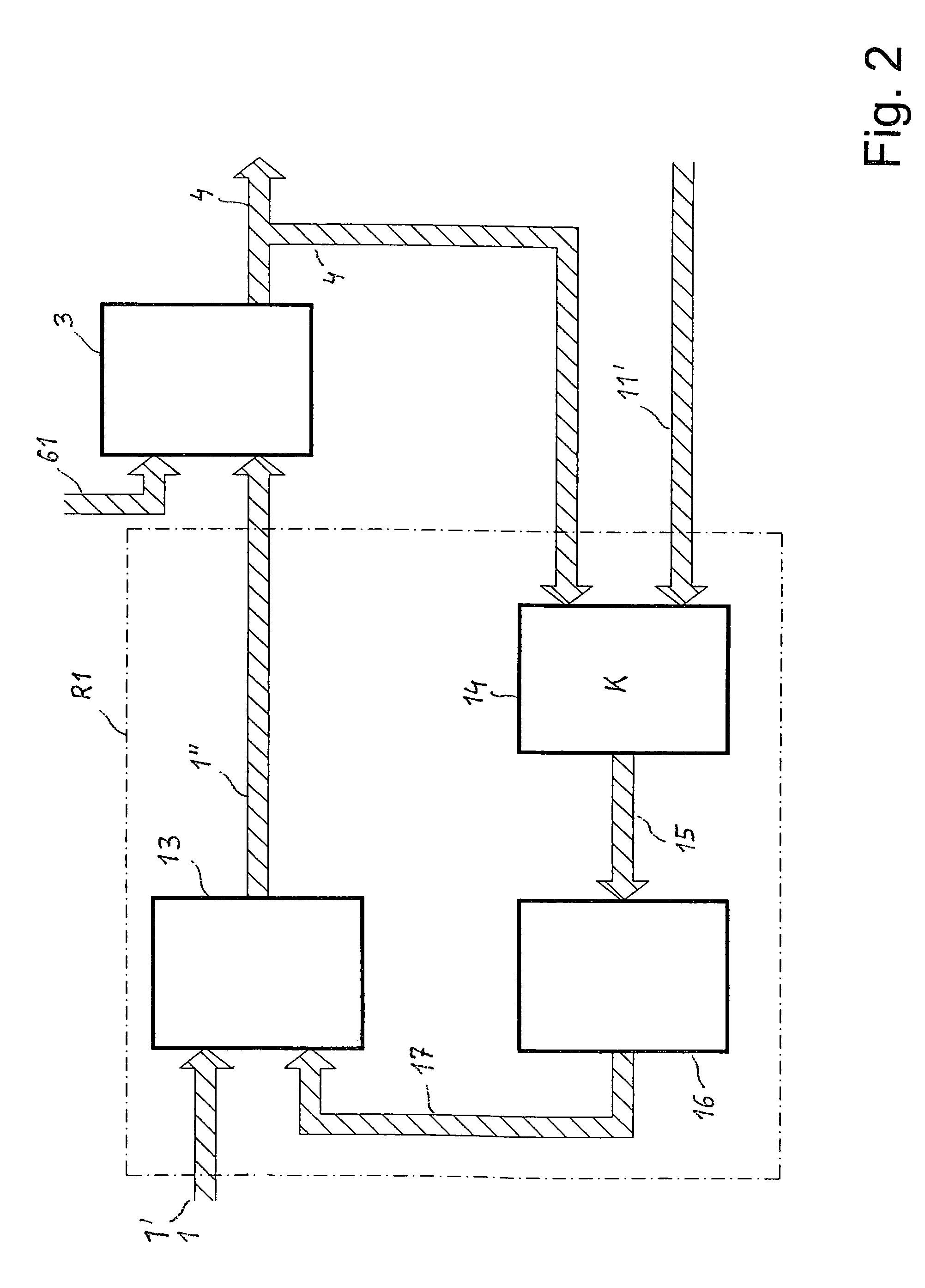
[0065]FIG. 2 shows the fundamental structure of a first embodiment R1 of a loop 2. In this embodiment, a regulator 13, a coding device 16, and a pulse error comparator 14 are provided. In this connection, the input data stream 1 or the input data stream 1′ of a predictor 12 are applied to the inputs of the regulator 13, as is the output signal 17 of the coder 16. The latter converts the digital signal sequence 15 that comes from the comparator 14 into an error data stream 17, which influences the regulator 13.
[0066]In this connection, an output signal of the mixer / coder circuit 3 and a signal 11 from the attenuator 10 (not shown in FIG. 2) is passed to the comparator 14, whereby the attenuator 10 is preferably connected with the point 6′ of the amplifier stage. The comparator 14 can preferably be an XOR link. The coding device 16 can be a time-limited up / down counter.
[0067]The regulator 13 generates an output data stream 1″ from the input data stream 1 or the data stream 1′ and the ...
second embodiment
[0079]2.2 Second Embodiment of Invention (V2)
[0080]The amplifier stage V2 according to FIG. 5 differs from the amplifier stage V3 according to FIG. 6 in that instead of the loop R3, a loop R2 is provided. The remainder of the structure of the amplifier stage V2 is the same as that of the amplifier stage V3.
[0081]Variations in the supply voltage of the D amplifier 5 can also be detected and regulated out by means of the loop R2. In this way, the voltage source of the D amplifier 5 can be structured in simple manner. The computing capacity for the comparator 19 and the regulator 13 can be implemented in a microprocessor, in rather slow manner, or quickly in a hard-wired computing circuit, in a circuit-programmable IC, whereby a pulse pattern correction is also possible.
third embodiment
[0082]2.3 Third Embodiment of Invention (V4)
[0083]The amplifier stage V4 in FIG. 7 differs from the amplifier stage V3 in that in addition, a loop R2 is provided, which is switched between the loops R3 and R1. In this connection, the output voltage of the amplifier stage V4 is fed back to the loop R3 by way of the A / D converter 20′, which generates a data stream 21′ from the output voltage 31.
[0084]The signal sequence 6 is fed back by way of the converter 20, which generates a data stream from the amplified signal sequence 6, which data stream is applied to the loop R2, which follows the loop R3, on the one hand. Furthermore, the signal sequence 6 is fed back to the loop R1, which follows the loop R2, by way of an attenuator 10 that generates a signal sequence 11.
[0085]The loop R3 regulates in accordance with the output voltage 31, and thereby reduces the demands on the converter 7. The timing element 22 of the loop R3 can be implemented in significantly simpler manner and with high...
PUM
 Abstract
Description
Claims
Application Information