

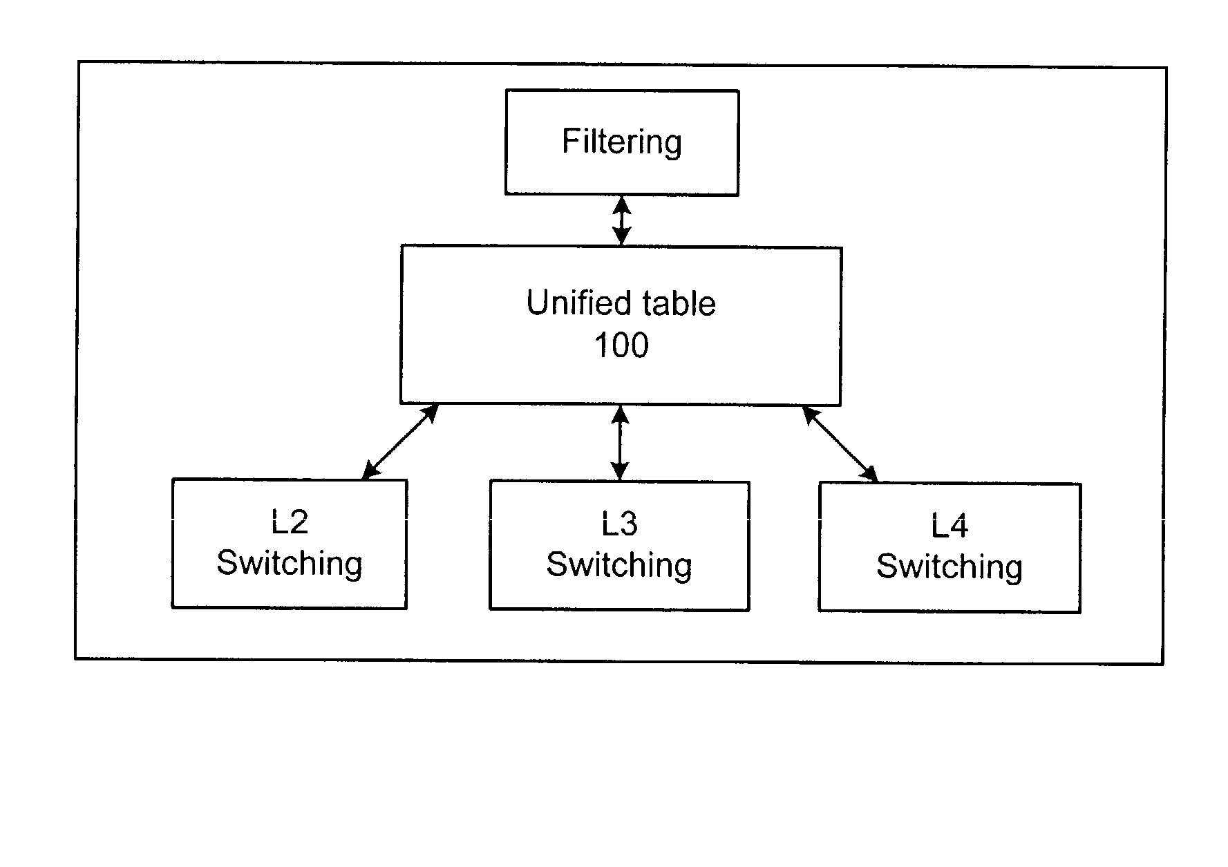
Unified table for L2, L3, L4, switching and filtering
a technology of switching and filtering, applied in the field of new switching architecture, can solve the problems of increasing design requirements, increasing design constraints, and relatively slow conventional dynamic random access memory (dram)
- Summary
- Abstract
- Description
- Claims
- Application Information
AI Technical Summary
Problems solved by technology
Method used
Image

Examples
Embodiment Construction
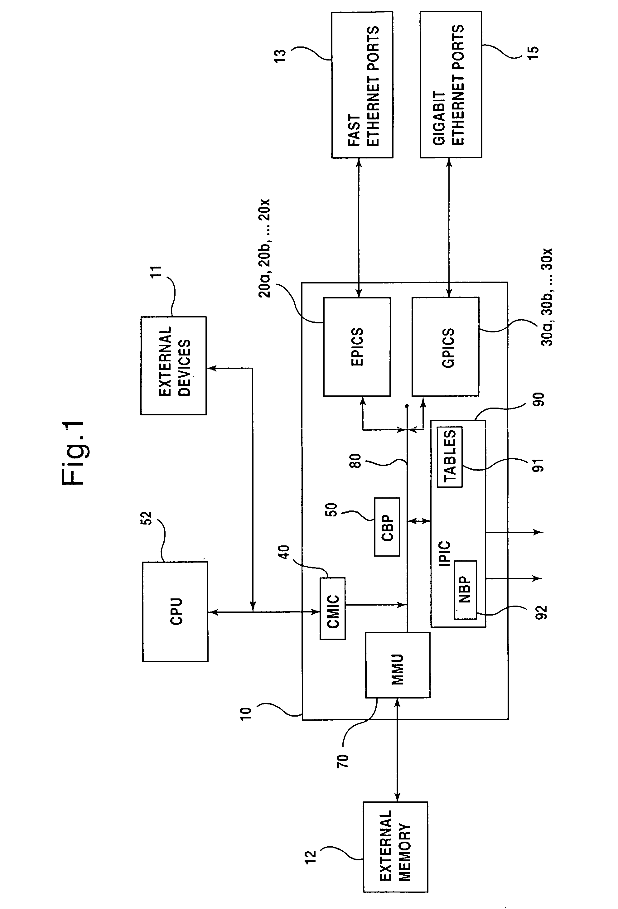
[0042]FIG. 1 illustrates a configuration wherein a switch-on-chip (SOC) 10, in accordance with the present invention, is functionally connected to external devices 11, external memory 12, fast ethernet ports 13, and gigabit ethernet ports 15. For the purposes of this embodiment, fast ethernet ports 13 will be considered low speed ethernet ports, since they are capable of operating at speeds ranging from 10 Mbps to 100 Mbps, while the gigabit ethernet ports 15, which are high speed ethernet ports, are capable of operating at 1000 Mbps. External devices 11 could include other switching devices for expanding switching capabilities, or other devices as may be required by a particular application. External memory 12 is additional off-chip memory, which is in addition to internal memory which is located on SOC 10, as will be discussed below. CPU 52 can be used as necessary to program SOC 10 with rules which are appropriate to control packet processing. However, once SOC 10 is appropriatel...
PUM
 Abstract
Description
Claims
Application Information