PLL circuit having a multi-band oscillator and compensating oscillation frequency

a multi-band oscillator and oscillator technology, applied in low noise amplifiers, phase-modulated carrier systems, instruments, etc., can solve problems such as no optimum one, temperature change of mobile phones, and thought to have errors, so as to achieve the effect of reducing the occupied area

Inactive Publication Date: 2006-09-05
GOOGLE TECH HLDG LLC +2
View PDF17 Cites 61 Cited by
  • Summary
  • Abstract
  • Description
  • Claims
  • Application Information

AI Technical Summary

Benefits of technology

[0012]In such a mobile phone capable of handling the multiple bands, the PLL circuit is an indispensable technology for obtaining a local oscillation signal having an optional frequency and the PLL circuit must be operated at a frequency based on the mobile phone to be used. A PLL circuit using a VCO that has multiple oscillation frequency bands and thus has a wide frequency range has been already proposed. This PLL circuit can compensate for the fluctuation of the VCO due to the variance of manufacture, by using the calibration function of its own. More specifically, even if the oscillation frequency of each band is not known exactly because of the variance of devices manufactured, the use of a automatic calibration function and an automatic band selection function make it possible to select the appropriate band.
[0019]Therefore, an object of the present invention is to provide a semiconductor integrated circuit device for communication such as an RFIC or the like having a PLL circuit or the like that controls a VCO having multiple oscillation frequency bands and that is capable of realize the compensation of operation due to temperature change, the inhibition of increase in the chip area, and the ensurement of the performance margin, with taking the products such as an RFIC or the like in consideration.
[0026](4) The present invention performs calibration in such a state that the PLL circuit is a closed loop, and oscillates and operates the VCO at a target frequency to measure this tuning voltage per each of frequency bands of the VCO, and selects a frequency band having a value that is near a threshold value corresponding to the target frequency. Or, the present invention selects a frequency band that is within a range between two threshold values corresponding to the target frequency. By such a constitution, in the PLL circuit in which the switching of the frequency band that has been once determined is not required, the occupied area can be reduced.
[0027](5) The present invention has a memory circuit for memorizing tuning sensitivity information showing dependence of frequency relative to a tuning voltage per each of frequency bands of the VCO, and controls a current value of the charge pump at the time of selecting each of the frequency bands of the VCO, in order to compensate for the dependence of the frequency relative to the tuning voltage on the basis of the tuning sensitivity information memorized in the memory circuit when the selected frequency band is compensated for. By such a constitution, in the case where the sensitivity of the frequency differs relative to the tuning voltage depending on the frequency band, the bandwidth of the PLL circuit can be compensated for to become constant by switching the current of the charge pump.

Problems solved by technology

Therefore, the calibration table constructed by the automatic calibration at the time of switch-on depends on temperature and so comes to no optimum one.
More specifically, after the switch-on, the temperature of the mobile phone changes as the temperature of the circuit therein increases, and even the date according to the calibration table constructed after the switch-on is thought to have some error.
As a result, there is a possibility that the optimum band can not be selected at the time of the automatic band selection.

Method used


Image

  • PLL circuit having a multi-band oscillator and compensating oscillation frequency
  • PLL circuit having a multi-band oscillator and compensating oscillation frequency
  • PLL circuit having a multi-band oscillator and compensating oscillation frequency

Examples


Embodiment Construction

[0059]Hereinafter, embodiments of the present invention will be described in detail based on the accompanying drawings. Note that components having the same function are denoted by the same reference symbol throughout all the drawings for describing the embodiments, and the repetitive description thereof will be omitted.

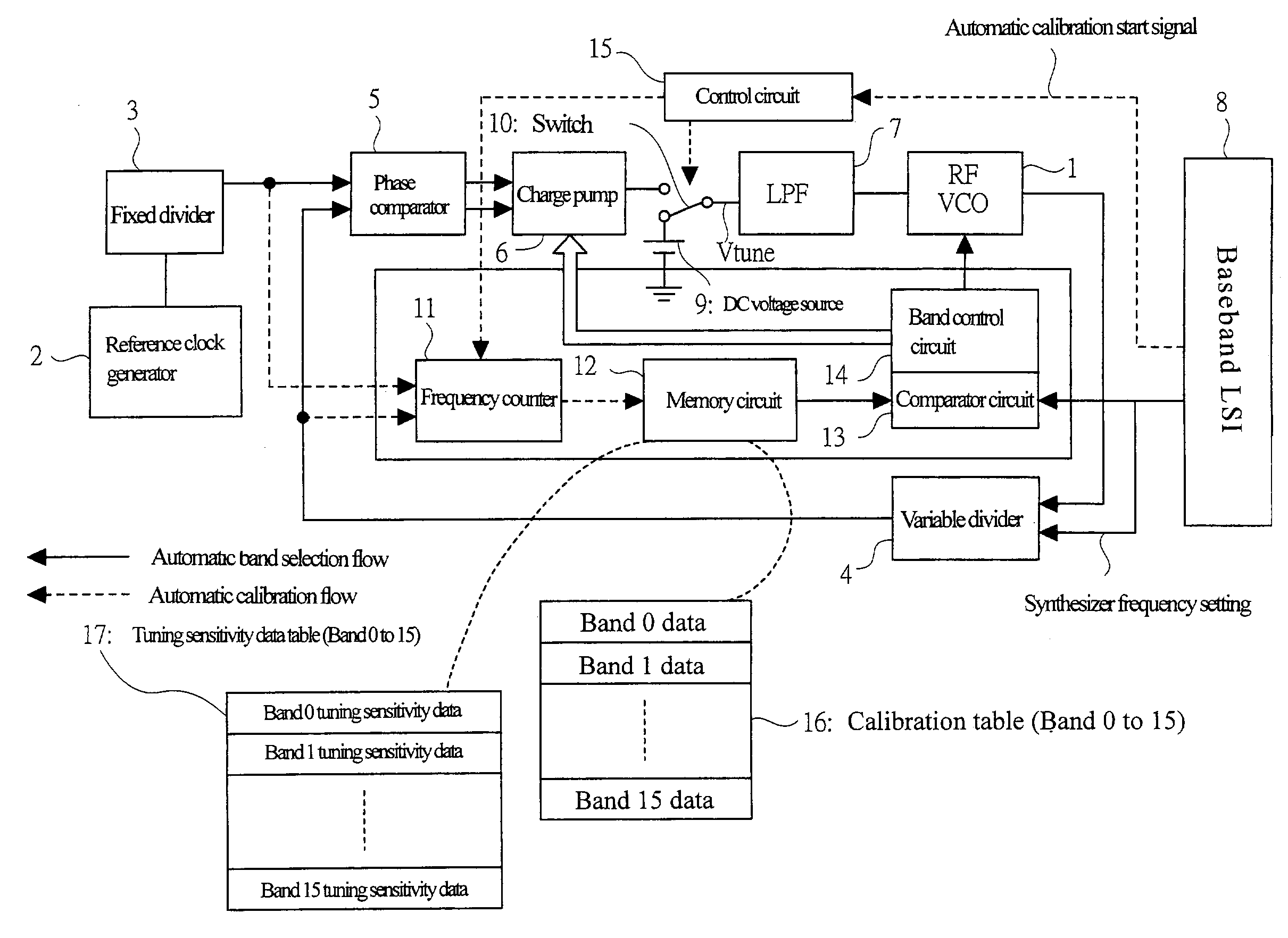
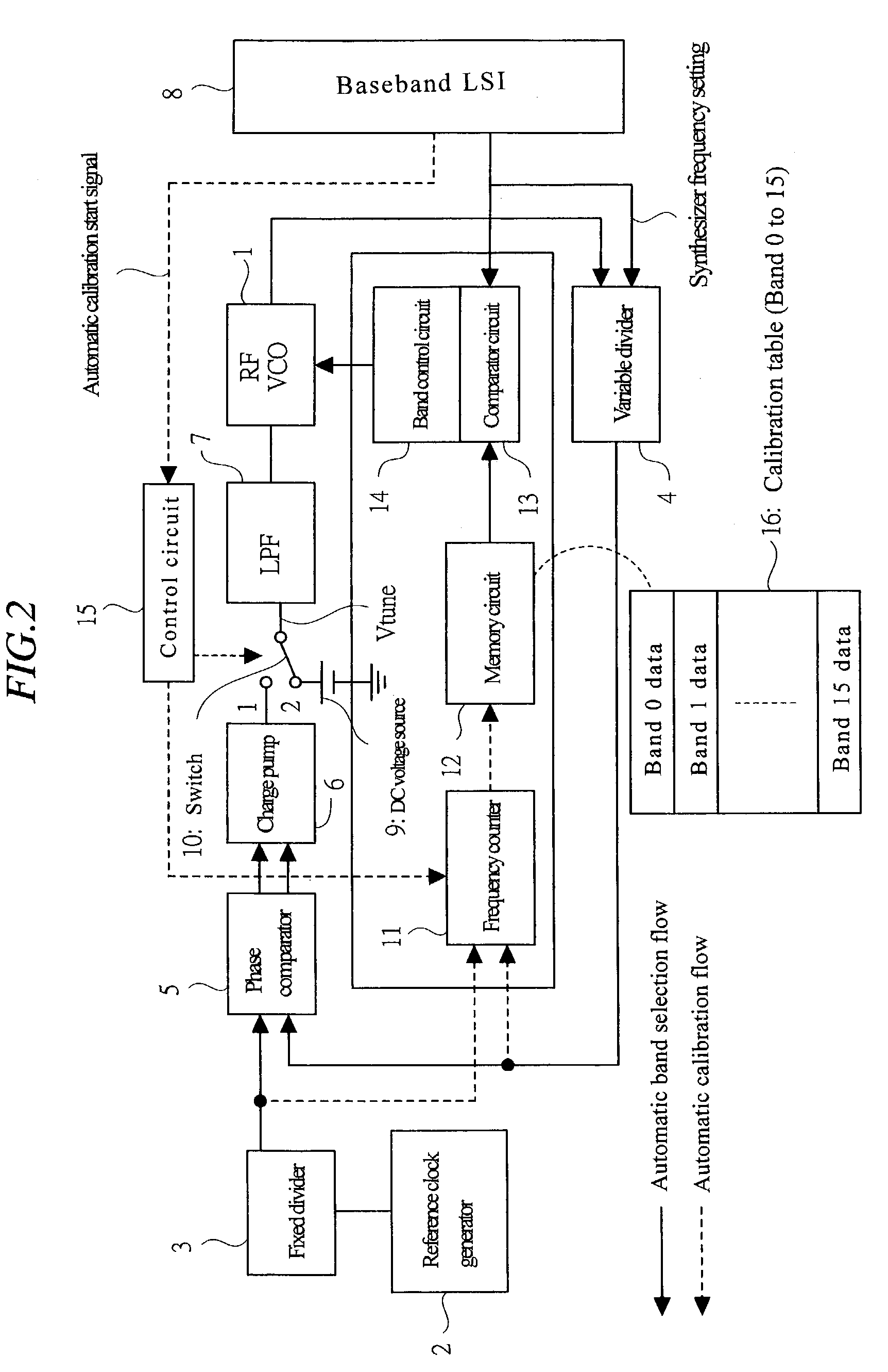
[0060]A PLL circuit to which the present invention is applied is used as a PLL synthesizer for controlling the VCO having multiple oscillation frequency bands. The PLL circuit has an automatic calibration function including a calibration at the time of switch-on and a recalibration after the switch-on, and an automatic band selection function for selecting an optimum oscillation frequency band based on a target frequency. Also, the PLL circuit can achieve the following: 1. Operating compensation due to temperature change, 2. Inhibition of the increase in the chip area, and 3. Ensurement of a performance margin. Each of them will be described below.

[0061]1. Operating ...


PUM


Abstract

A semiconductor integrated circuit device for communication is provided with a PLL circuit or the like formed therein, the PLL circuit which is capable of realizing the compensation of fluctuation due to temperature change, the inhibition of increase in the chip area and the ensurement of the performance margin, and which controls a VCO having multiple oscillation frequency bands. In the case where automatic calibration is performed by switching a switch to a side of a DC voltage source in the PLL circuit using a VCO having multiple oscillation bands, a tuning voltage (Vtune) of an RFVCO is fixed to a voltage value of a DC voltage source. However, since a temperature characteristic of canceling a VCO oscillation frequency is given to the DC voltage source, it is possible to minimize the influence on the band selection when a calibration table comes to no optimum one.

Description

CROSS-REFERENCES TO RELATED APPLICATIONS[0001]The following applications, including this one, are being filed concurrently, and the disclosure of the other applications are incorporated by reference into this application in their entirety for all purposes:[0002]U.K. Patent Application No. 0212737.1 (filed on May 31, 2002) entitled “APPARATUS FOR RADIO TELECOMMUNICATION SYSTEM AND METHOD OF BUILDING UP OUTPUT POWER”[0003]U.K. Patent Application No. 0212725.6 (filed on May 31, 2002) entitled “A COMMUNICATION SEMICONDUCTOR INTEGRATED CIRCUIT, A WIRELESS COMMUNICATION APPARATUS, AND A LOOP GAIN CALIBRATION METHOD”[0004]U.K. Patent Application No. 0212729.8 (filed on May 31, 2002) entitled “TRANSMITTER AND SEMICONDUCTOR INTEGRATED CIRCUIT FOR COMMUNICATION”[0005]U.K. Patent Application No. 0212723.1 (filed on May 31, 2002) entitled “SEMICONDUCTOR INTEGRATED CIRCUIT FOR COMMUNICATION, RADIO-COMMUNICATIONS APPARATUS, AND TRANSMISSION STARTING METHOD”[0006]U.K. Patent Application No. 021273...

Claims


Application Information

Patent Timeline
Patent Type & Authority Patents(United States)
IPC IPC(8): H04B1/06H03F1/02H03F1/34H03G3/30H03L7/099H03L7/187H04B1/04H04L27/00H04L27/20H04L27/36
CPCH03F1/0211H04L27/368H03F1/0272H03F1/345H03G3/3042H03G3/3047H03L7/0898H03L7/099H03L7/187H04L27/0008H04L27/2017H04L27/2071H04L27/361H03F1/0266H03F2200/294H03F2200/372H04B2001/0416
Inventor UOZUMI, TOSHIYATANAKA, SATOSHIKASAHARA, MASUMIOOSAWA, HIROTAKAKIMURA, YASUYUKIHENSHAW, ROBERT ASTLE
Owner GOOGLE TECH HLDG LLC
Why Eureka
Try Eureka