Memory device

Inactive Publication Date: 2006-09-05
FUJIFILM CORP
View PDF24 Cites 15 Cited by
  • Summary
  • Abstract
  • Description
  • Claims
  • Application Information

AI Technical Summary

Benefits of technology

[0006]Accordingly, an object of the present invention is to shorten data processing time.

Problems solved by technology

Enlarging the bus width, however, may result in more complicated wiring.
However, such processing is comparatively complicated.

Method used


Image

  • Memory device
  • Memory device
  • Memory device

Examples


Embodiment Construction

[0017]A preferred embodiment of the present invention will now be described with reference to the drawings.

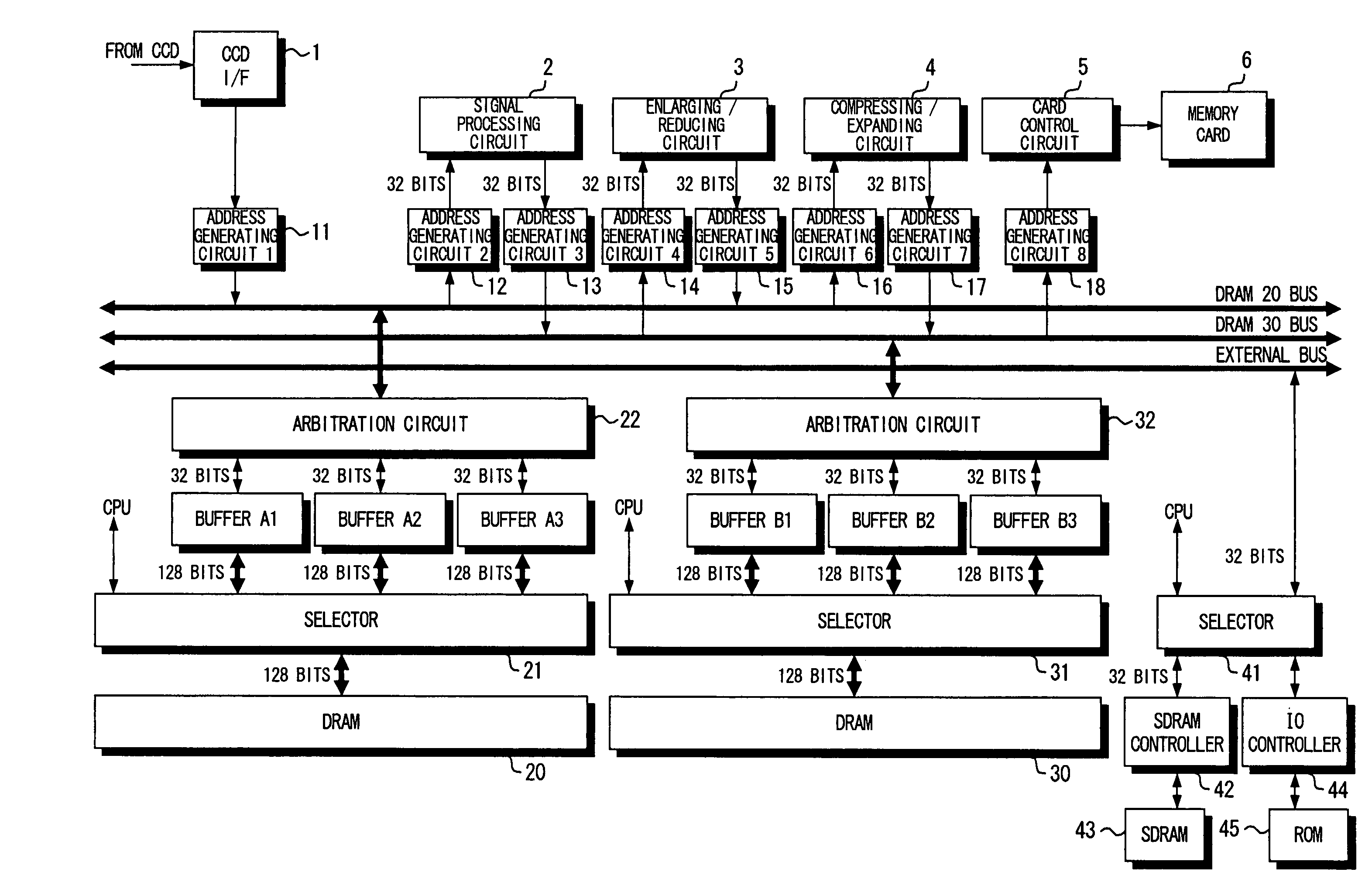
[0018]FIG. 1, which illustrates a preferred embodiment of the present invention, is a block diagram showing part of the electrical structure of a digital still camera.

[0019]The digital still camera includes a first DRAM (dynamic random-access memory) 20 and a second DRAM 30 for storing image data temporarily. A first buffer circuit A1, second buffer circuit A2 and third buffer circuit A3, each of which stores image data temporarily, are connected to the first DRAM 20 via a selector 21 by means of buses (a data bus for a data memory and a first data bus). A first arbitration circuit 22 is connected to the first to third buffer circuits A1 to A3 via a bus having a bus width of 32 bits. The first arbitration circuit 22 decides to and from which of first to third buffer circuits A1 to A3 image data is to be written and read. Similarly, a first buffer circuit B1, second buffer circu...


PUM


Abstract

A memory device is so adapted that data processing time is not prolonged even when there is little bus width. A DRAM is connected to first to third buffer circuits by buses, which have a bus width of 128 bits, via a selector. The first to third buffer circuits are connected to a circuit such as a signal processing circuit by buses having a bit width of 32 bits. Since part of the circuitry is connected by buses having a bit width of 32 bits, the wiring is simple. By executing various processing in parallel, it is possible to prevent prolongation of the time required to record image data on a memory card.

Description

BACKGROUND OF THE INVENTION[0001]1. Field of the Invention[0002]This invention relates to a memory device.[0003]2. Description of the Related Art[0004]In order to shorten write time for writing data to a memory and read-out time for reading data out of the memory, it will suffice to enlarge the bus width of the data bus connected to the memory. Enlarging the bus width, however, may result in more complicated wiring.[0005]Data processing time may be shortened by accessing a memory more efficiently, as disclosed in, e.g., the specification of Japanese Patent Application No. 10-53083. However, such processing is comparatively complicated.DISCLOSURE OF THE INVENTION[0006]Accordingly, an object of the present invention is to shorten data processing time.[0007]According to the present invention, the foregoing object is attained by providing a memory device comprising a data memory to and from which data is input and output via a data bus for a data memory; and a plurality of buffer circui...

Claims


Application Information

Patent Timeline
IPC IPC(8): G06F13/40G06F13/12G06F15/16G06F3/00G09G5/399G06F13/20G06F12/00G06F12/04G11C7/10G11C11/22
CPCG11C7/10G11C7/1012G11C7/1006
Inventor FUNAMOTO, KENJI
Owner FUJIFILM CORP
Why Eureka
Try Eureka