Method and apparatus for collecting defect images

a technology of defect image and method, applied in the direction of material analysis using wave/particle radiation, semiconductor/solid-state device testing/measurement, instruments, etc., can solve the problems of defect present in the device, high failure rate of such a product, and degradation of yield, so as to achieve efficient effect of suitable observation

Active Publication Date: 2006-09-12
HITACHI HIGH-TECH CORP
View PDF6 Cites 10 Cited by
  • Summary
  • Abstract
  • Description
  • Claims
  • Application Information

AI Technical Summary

Benefits of technology

[0011]The present invention provides a means capable of efficiently effecting suitable observations even on a defect on the top surface and a defect below a film of an object being inspected.
[0014]According to the present invention, when a defect is observed using a SEM on the basis of data concerning the position of a defect, which is outputted from a defect inspecting device by an optical means, the defect can be observed efficiently even when the defect exists below an optically transparent film.

Problems solved by technology

When a foreign substance and anomalies in appearance, such as a break in wiring, etc., occur on a thin-film device due to imperfections and problems involving the manufacturing conditions of the processing equipment, the probability that a failure will occur in such a product becomes high, thus causing a degradation of the yield.
When the number of defects exceeds a preset reference value, it is judged that a defect is present in the device.
Estimating the cause of the defects a from defect's visual information depends on high-level judgment of an analyzer, and differences among individuals and the time necessary for such a judgment present problems.
Therefore, a defect that exists below the film is also detected.
Therefore, when no defect is observed during a detailed review using a SEM adapting to the defect detected by the defect inspecting device, a decision can not be made as to whether the results indicate disinformation or a below-film defect.
However, a technique that makes it possible to obtain suitable observations that are compatible between a defect observation of the top surface and an internal observation has not yet been disclosed.
However, a method of bringing a review work operation into high efficiency according to the circumstances of a target defect has not been disclosed therein.

Method used


Image

  • Method and apparatus for collecting defect images
  • Method and apparatus for collecting defect images
  • Method and apparatus for collecting defect images

Examples


Embodiment Construction

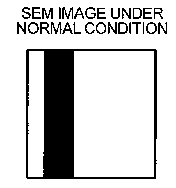
[0033]Although embodiments of the present invention to be described hereinafter concern devices that observe defects and analyze elements, such as semiconductor wafers, the present invention is not limited to such devices, but may consist of other types of devices.

[0034]Preferred embodiments of the present invention will be described hereinafter with reference to the accompanying drawings.

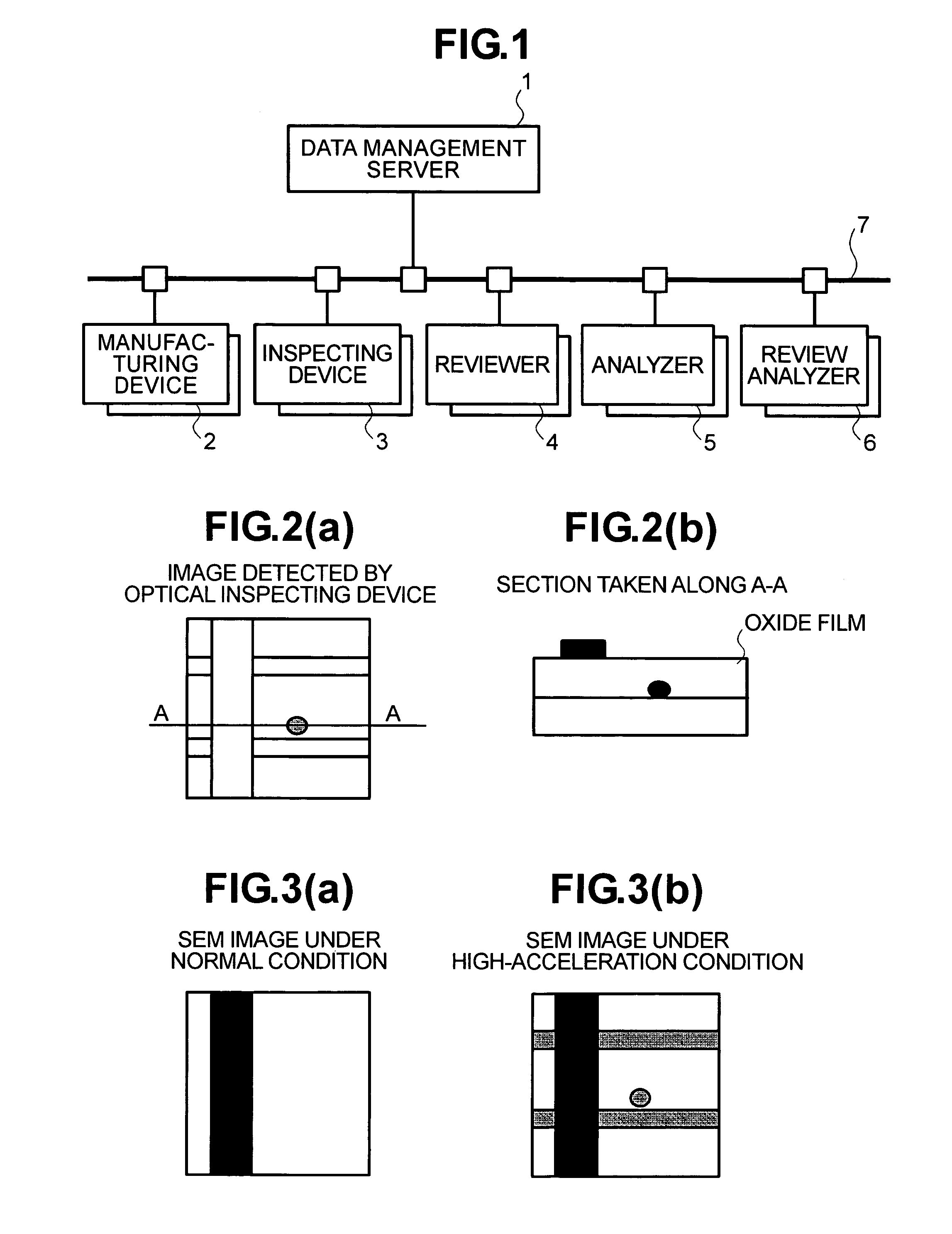
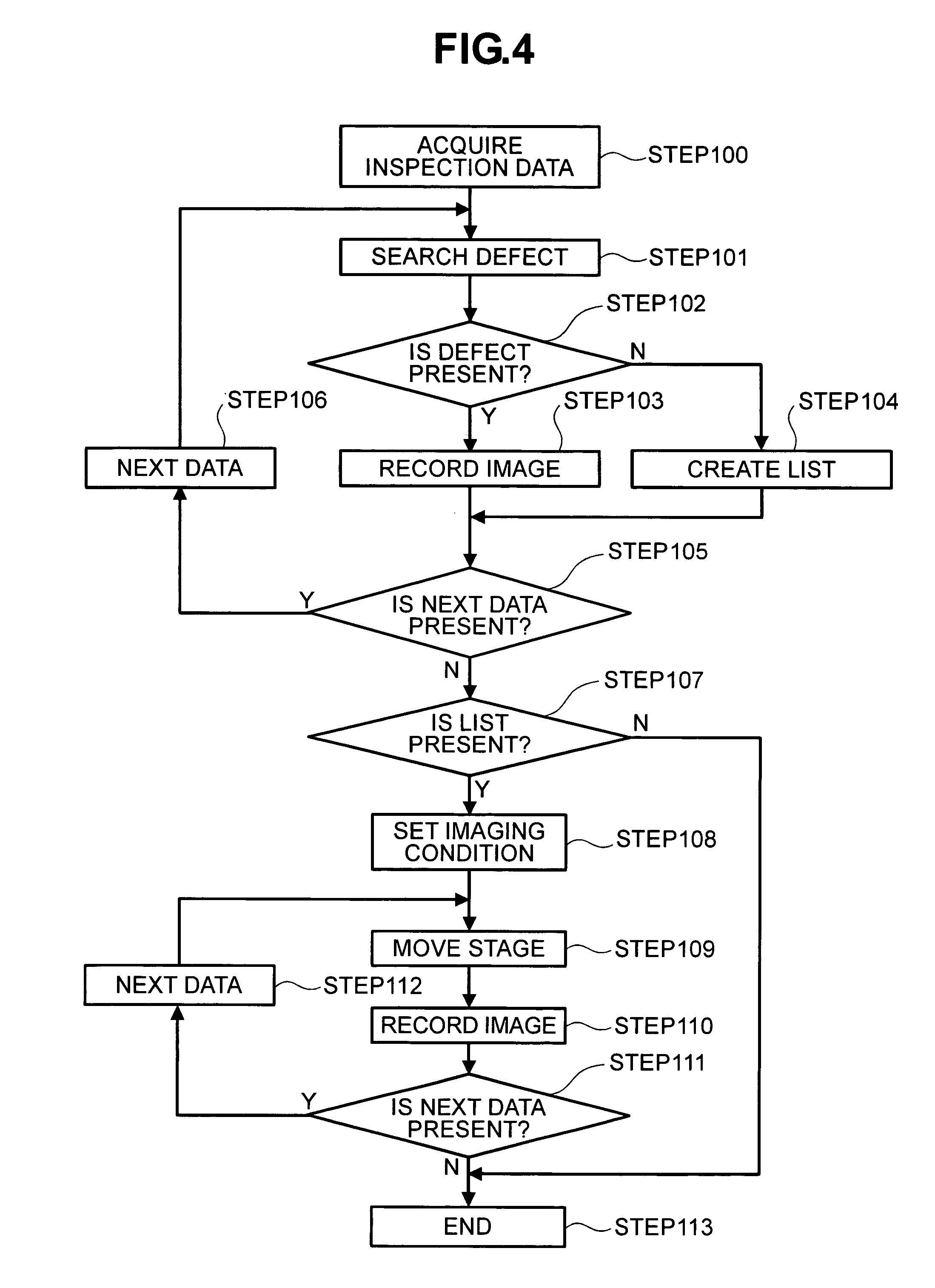
[0035]One specific example illustrative of the respective devices used in a wafer production line and their connecting configuration will first be described with reference to FIG. 1. In FIG. 1, the production line has a data management server 1, a semiconductor wafer manufacturing device 2, an inspecting device 3, a reviewer 4, an analyzer 5, a review analyzer 6, and a network 7.

[0036]In the production line, the semiconductor wafer manufacturing device 2, the inspecting device 3, the reviewer 4, the analyzer 5 and the review analyzer 6 are connected to one another by the data management server 1 an...


PUM

PropertyMeasurementUnit
accelerating voltageaaaaaaaaaa

Abstract

To acquire defect images even when a defect exists below an optically transparent film, an electron optical system of an electron microscope is set to a first imaging condition. A defect position of a specimen is set so as to fall within the visual field of the electron microscope, using position data of a defect of the specimen. The position of the defect is imaged by the electron microscope set to the first imaging condition to obtain a first image corresponding to the defect position. The first image is processed to determine whether a defect exists. The electron optical system is then set to a second imaging condition on the basis of the result of determination. A point imaged under the first imaging condition is imaged by the electron microscope set to the second imaging condition to acquire a second image corresponding to a defect position.

Description

BACKGROUND OF THE INVENTION[0001]The present invention relates in general to a method to be used for collecting defect images of a foreign substance and a defect generated in a thin film device manufacturing process on the basis of inspection information, and an apparatus for use in carrying out the method.[0002]The production of thin-film devices, such as a semiconductor, a liquid crystal display device, a hard disk magnetic head, etc., involves a large number of processes. The number of process steps for performing such work reaches several hundreds of process steps on occasion.[0003]When a foreign substance and anomalies in appearance, such as a break in wiring, etc., occur on a thin-film device due to imperfections and problems involving the manufacturing conditions of the processing equipment, the probability that a failure will occur in such a product becomes high, thus causing a degradation of the yield. Thus, in order to maintain a desired yield and to provide improvements i...

Claims


Application Information

Patent Timeline
Patent Type & Authority Patents(United States)
IPC IPC(8): G01N23/00G21K7/00H01J37/28G01N23/225H01L21/66
CPCH01J37/241H01J37/263H01J37/28H01J37/265H01J2237/2817H01J2237/2809
Inventor OBARA, KENJIHONDA, TOSHIFUMIKUBO, TOSHIRO
Owner HITACHI HIGH-TECH CORP
Why Eureka
Try Eureka