Multilaser device for receiving a plurality of back beams by a common sensor

a back beam and laser diode technology, applied in semiconductor lasers, instruments, electrographic processes, etc., can solve the problems of uneven converging properties of spots, uneven image density, and deterioration of printing quality, so as to reduce heat interference among a plurality of laser diodes.

Inactive Publication Date: 2006-09-12
CANON KK
View PDF3 Cites 9 Cited by
  • Summary
  • Abstract
  • Description
  • Claims
  • Application Information

AI Technical Summary

Benefits of technology

[0007]It is an object of the present invention to provide a multilaser device in which heat interference among a plurality of laser diodes is reduced.

Problems solved by technology

In the image forming apparatus, such a reduction in the quantity of emitted light results in the uneven density of an image and deteriorates the quality of printing.
As one of methods of solving the above-noted problem, there is a method of carrying a plurality of laser diode chips to thereby form a multibeam, but this method gives rise to the problem that depending on the mounting accuracy of the laser diode chips in a semiconductor laser, the distance from a light emitting point to a photosensitive drum differs among the laser diode chips, whereby the converging property of a spot becomes uneven.

Method used


Image

  • Multilaser device for receiving a plurality of back beams by a common sensor
  • Multilaser device for receiving a plurality of back beams by a common sensor
  • Multilaser device for receiving a plurality of back beams by a common sensor

Examples


second embodiment

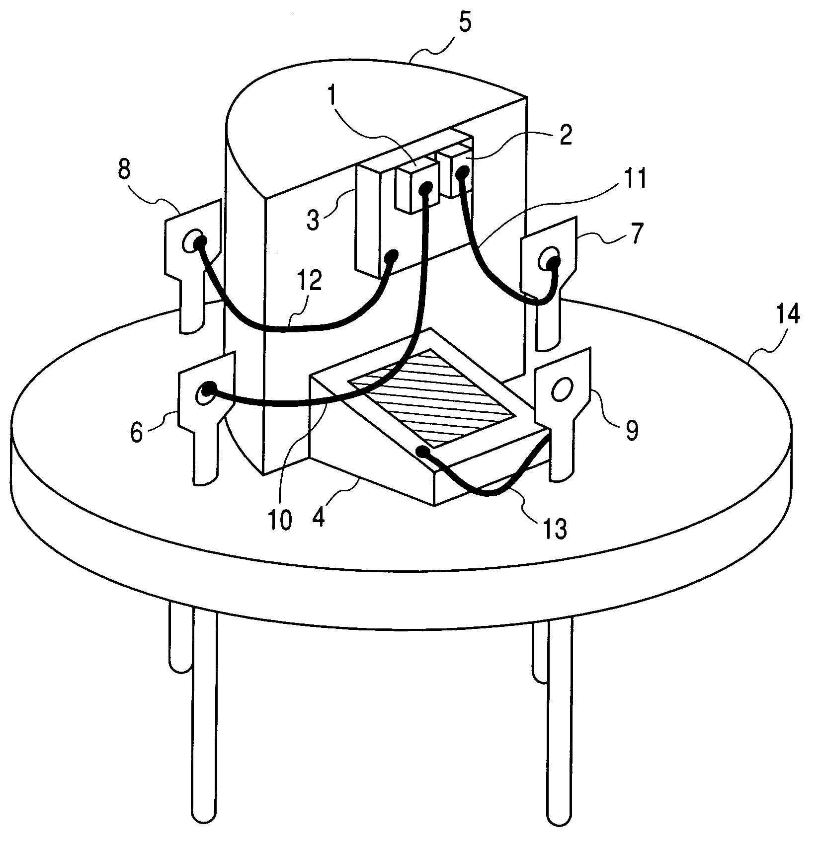
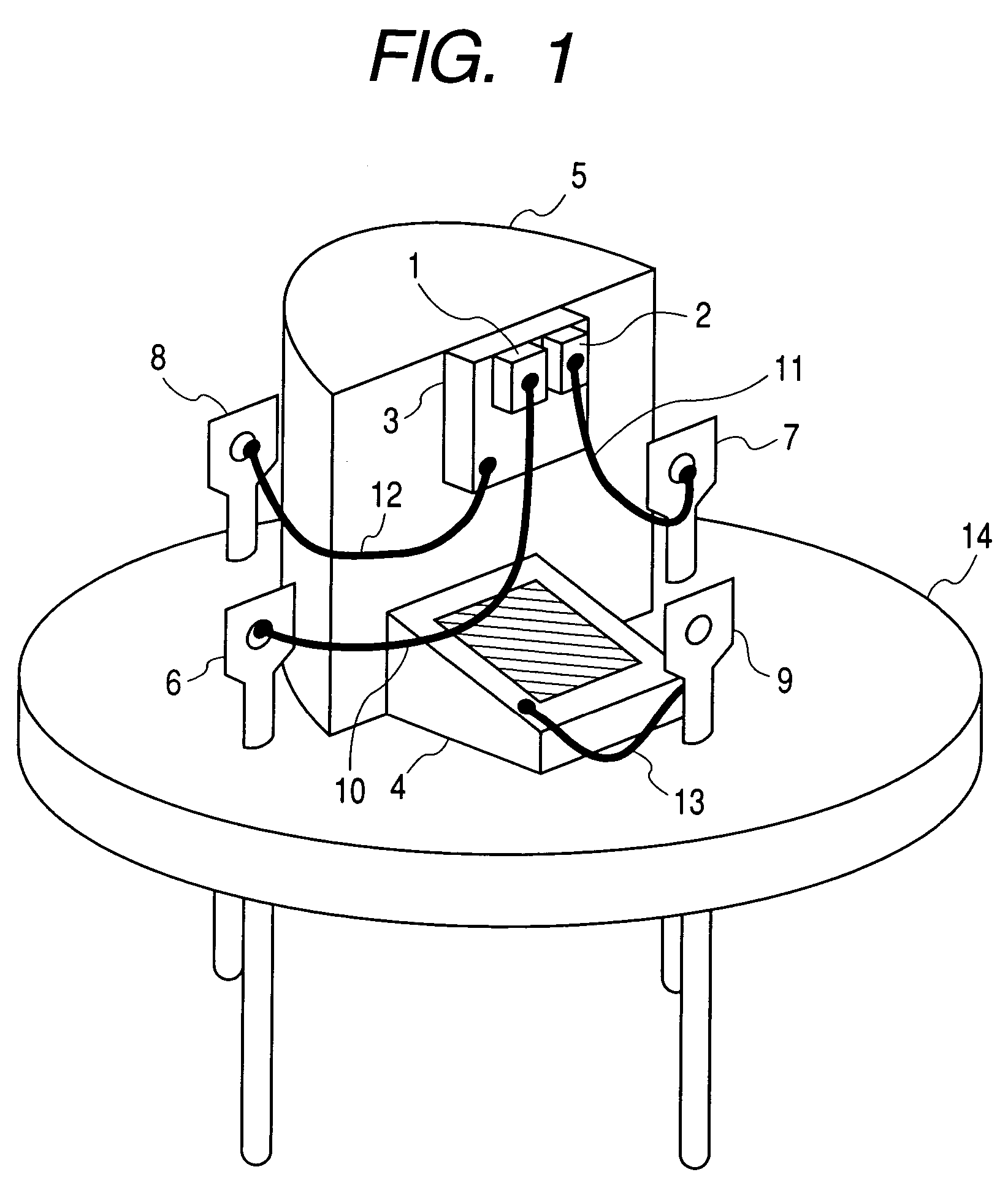
[0026]FIG. 4 is a schematic view of the internal structure of the semiconductor multibeam laser illustrating second and third embodiments of the present invention. The part surface of the stem 14 provides a reference surface when the semiconductor multibeam laser apparatus is mounted on a laser driving unit 31. The LD chip a 1 and the LD chip b 2 are mounted on the sub-mount 3 so that the distance to the light emitting point of the LD chip a 1 and the distance to the light emitting point of the LD chip b 2 may be equal to each other relative to the reference surface of the stem 14.

[0027]Assuming here that the distance to the light emitting point of the LD chip a 1 relative to the reference surface of the stem 14 is Z1 and the distance to the light emitting point of the LD chip b 2 relative to the reference surface of the stem 14 is Z2, the relative difference in the positional accuracy of the light emitting points is defined as shown by the following expression (1):

relative differen...


PUM


Abstract

A multilaser device has a first laser chip and a second laser chip produced from one and the same wafer lot, a common back beam sensor for receiving a first back beam and a second back beam emitted from the first laser chip and the second laser chip, respectively, and a package containing the first laser chip, the second laser chip and the back beam sensor.

Description

BACKGROUND OF THE INVENTION[0001]1. Field of the Invention[0002]This invention relates to a multilaser device suitably used in an electrophotographic apparatus and emitting a plurality of laser beams.[0003]2. Description of Related Art[0004]A multibeam laser has heretofore been of a monolithic construction provided with a plurality of light emitting portions on a laser diode chip. In an image forming apparatus of an electrophotographic type, a plurality of beams are caused to scan by the use of this multibeam laser, and are applied onto a photosensitive drum to thereby effect latent image forming.[0005]In the above-described monolithic type, however, an electric current is supplied to one of the plurality of light emitting portions on the laser diode chip, whereby from the heat generation thereof, the threshold value electric currents of the other light emitting portions are increased and further, this leads to a reduction in the quantity of emitted light. This phenomenon is particu...

Claims


Application Information

Patent Timeline
Patent Type & Authority Patents(United States)
IPC IPC(8): H01S5/00B41J2/44G02B26/10G03G15/04H01S5/022H01S5/026H01S5/0683H01S5/40
CPCH01S5/02248H01S5/4025B41J2/442H01S5/0683H01L2224/48091H01S5/02212H01L2924/00014H01S5/02325
Inventor SEKI, YUICHI
Owner CANON KK
Why Eureka
Try Eureka