Wafer Having Thermal Circuit And Power Supplier Therefor

Inactive Publication Date: 2008-06-05
JOEUN TECH
View PDF9 Cites 4 Cited by
  • Summary
  • Abstract
  • Description
  • Claims
  • Application Information

AI Technical Summary

Benefits of technology

[0011]The present invention provides a wafer having a thermal circuit and power supplier therefor, in which the thermal circuit is installed in the wafer to self-heat the wafer, so that a temperature of a semiconductor device can be precisely controlled, and heating and cooling energies are greatly reduced through a direct heat exchange method, thus attaining high efficiency. Since the thermal circuit is directly installed in the wafer, it is structurally simple and the costs of production and installation can be notably reduced.
[0012]Also, the present invention provides a wafer having a thermal circuit and a power supplier therefor, which are very advantageous for optimization, miniaturization, simplification, and environmentally friendly production of a wafer heating / cooling system.
[0013]Furthermore, the present invention provides a wafer having a thermal circuit and power supplier therefor, in which a temperature measuring circuit is installed on a reverse surface of the wafer so that the amount of energy that acts on an actual semiconductor device or actual temperature can be accurately measured in real time.
[0015]In one embodiment, the thermal circuit may include a plurality of blocks, which are formed on a reverse surface of the wafer and correspond to at least one semiconductor device chip formed on a front surface of the wafer. In another embodiment, the thermal circuit may include a plurality of blocks from the center of a reverse surface of the wafer to the edge thereof, and an insulation groove may be formed between every two blocks to reduce thermal interference between the blocks.

Problems solved by technology

In addition to the multi-step heat exchange process, it is difficult to control heat conduction for each heat exchange process.
That is, owing to unstable heat convection in the air layer, it is very difficult to heat (cool) the semiconductor device disposed on the wafer to a desired temperature.
Thus, a lot of heating (cooling) energy is wasted so that the system's efficiency is deteriorated.
Further, because the conventional wafer heating (cooling) system is separately installed from the wafer and structurally complicated, it takes much time and cost to produce and install the system.
Also, in the conventional wafer heating system or cooling system, the heater is unnecessarily large-sized, a coolant, such as cooling water, is high-priced, and a variety of contaminants are generated, thus polluting the environment.
Meanwhile, a conventional wafer temperature measuring system also cannot precisely measure the amount of thermal energy that acts on the semiconductor device or actual temperature in real time because the system is separately installed from the wafer (e.g., an additional test wafer is used or a sensor is installed in vicinity of a wafer to measure temperature).

Method used


Image

  • Wafer Having Thermal Circuit And Power Supplier Therefor
  • Wafer Having Thermal Circuit And Power Supplier Therefor
  • Wafer Having Thermal Circuit And Power Supplier Therefor

Examples


Embodiment Construction

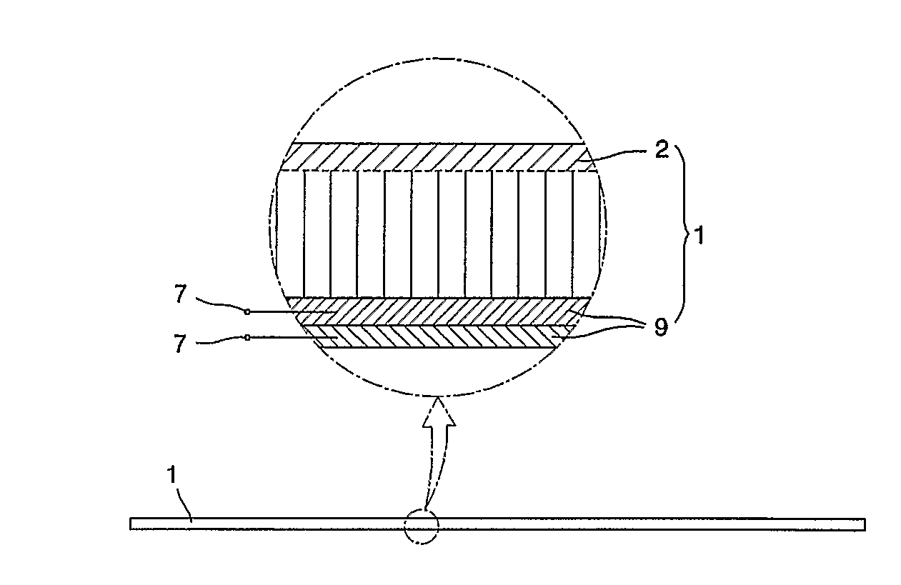
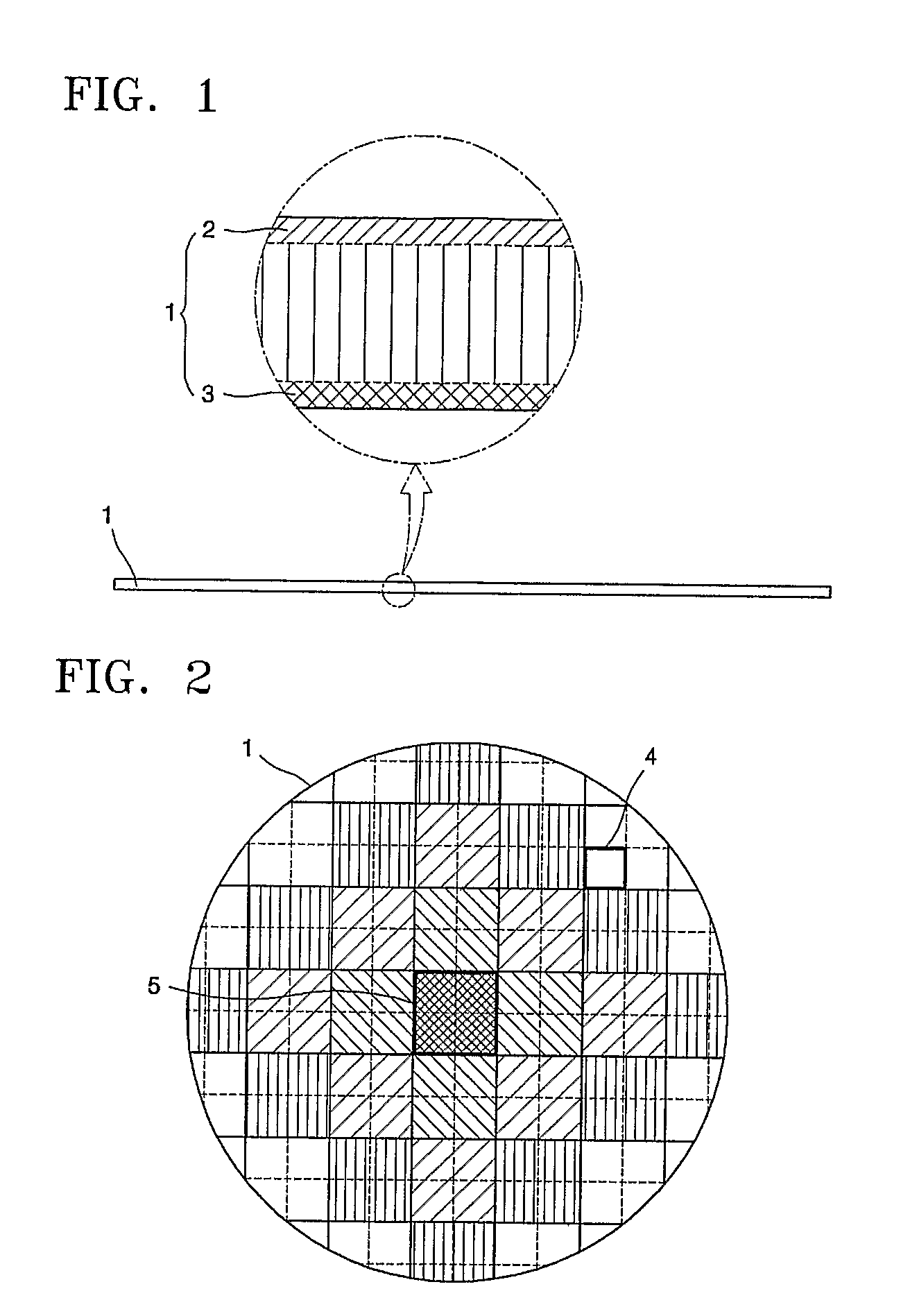
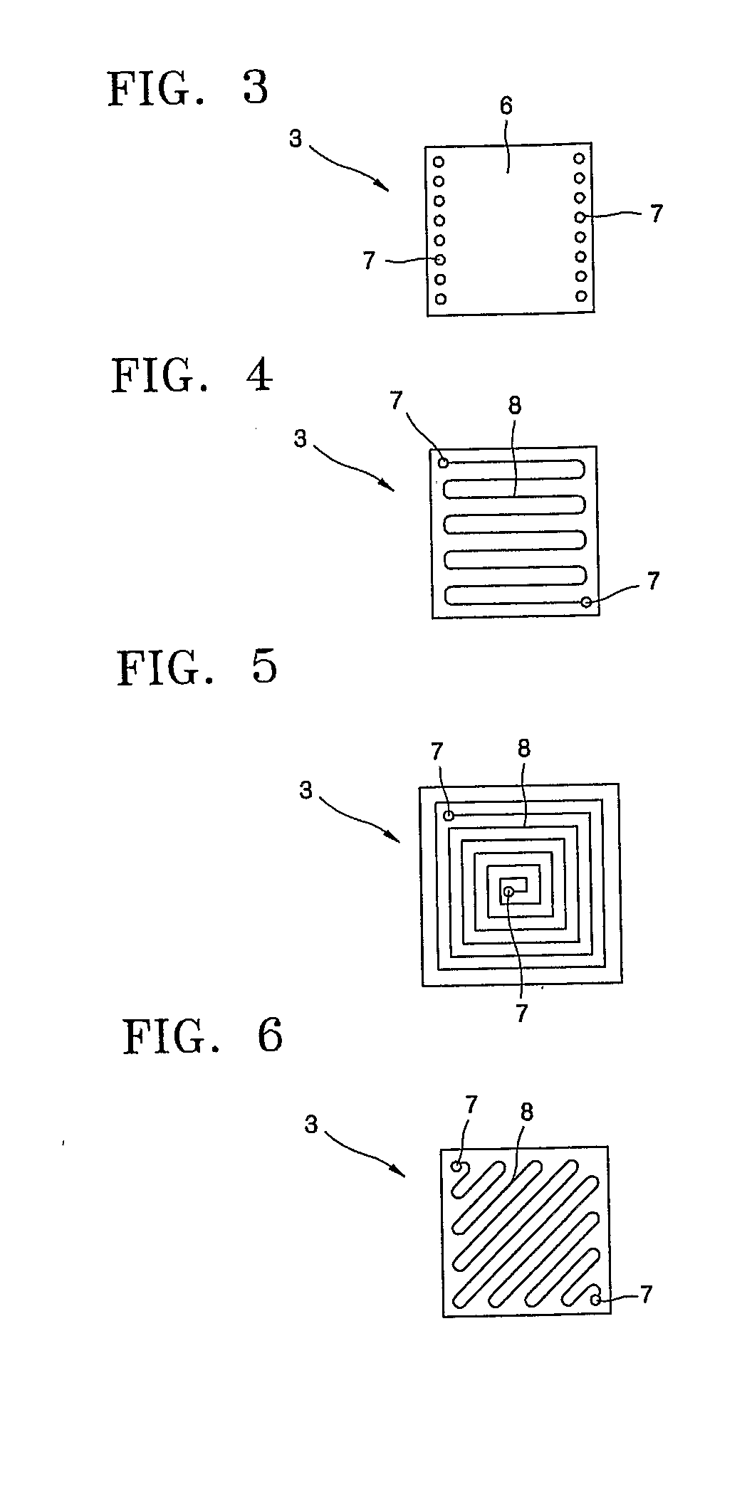
[0025]A wafer having a thermal circuit and power supplier therefor according to the present invention will now be described more fully hereinafter with reference to the accompanying drawings, in which exemplary embodiments of the invention are shown.

[0026]Referring to FIG. 1, a wafer 1 includes a thermal circuit 3 that is installed on a reverse surface of the wafer 1 to self-heat or self-cool the wafer in order to perform a heating process or cooling process on a semiconductor device 2 formed on the surface of the wafer 1 and exchanges heat with the semiconductor device 2. Thus, the thermal circuit 3 can directly exchange heat with the semiconductor device 2 formed on a top surface of the wafer 1.

[0027]Thus, since the thermal circuit 3 is installed in the vicinity of the semiconductor device 2, it can easily raise or drop the temperature of the semiconductor device 2 with small energy. Also, since heat is transmitted only through thermal conductance very precise heat control is poss...


PUM

PropertyMeasurementUnit
Temperatureaaaaaaaaaa
Forceaaaaaaaaaa
Poweraaaaaaaaaa

Abstract

Provided are a wafer having a thermal circuit and power supplier therefor, which enable the wafer to heat or cool itself without using any additional heating or cooling system. The wafer includes the thermal circuit that is installed on one side of the wafer to be capable of self-heating or self-cooling the wafer in order to perform a heating process or cooling process on a semiconductor device formed on the surface of the wafer and exchanges heat with the semiconductor device. Thus, a temperature of a semiconductor device can be precisely controlled, and heating and cooling energies are greatly reduced through a direct heat exchange method, thus attaining high efficiency. Since the thermal circuit is directly installed in the wafer, it is structurally simple and the costs of production and installation can be notably reduced. Also, the present invention is very advantageous for optimization, miniaturization, simplification, and environmentally friendly production of a wafer heating / cooling system. Furthermore, a temperature measuring circuit is installed on a reverse surface of the wafer so that the amount of energy that acts on an actual semiconductor device or actual temperature can be accurately measured in real time.

Description

TECHNICAL FIELD[0001]The present invention relates to a wafer having a thermal circuit and a power supplier therefor, and more particularly, to a wafer having a thermal circuit and power supplier therefor, which enable the wafer to be heated or cooled without any additional heating or cooling system.BACKGROUND ART[0002]In general, a semiconductor device is fabricated through a plurality of processes including an ion implantation process, a layer deposition process, a diffusion process, and a photolithography process. Among these processes, the photolithography process, which is carried out to form a desired pattern, is an essential process for the fabrication of the semiconductor device.[0003]In the photolithography process, a mask pattern or a reticle pattern is formed on the semiconductor device in order to selectively define a region to be doped and a region to be protected. Conventionally, such a photolithography process includes a coating process in which a photoresist is dropp...

Claims


Application Information

Patent Timeline
IPC IPC(8): H01L23/34
CPCH01L21/67103H01L23/34H01L23/345H01L23/38H01L2924/0002H01L2924/00H01L21/00H01L21/324
Inventor LEE, YOUNG-WEON
Owner JOEUN TECH
Why Eureka
Try Eureka