Electrochemical fabrication methods including use of surface treatments to reduce overplating and/or planarization during formation of multi-layer three-dimensional structures

a three-dimensional structure and fabrication method technology, applied in the direction of additive manufacturing apparatus, liquid/solution decomposition chemical coating, coating, etc., can solve the problem of destructive separation of masking material from substrate, and achieve the effect of reducing the formation time of layers

Inactive Publication Date: 2006-09-19
MICROFAB
View PDF24 Cites 45 Cited by
  • Summary
  • Abstract
  • Description
  • Claims
  • Application Information

AI Technical Summary

Benefits of technology

[0035]It is an object of some embodiments of various aspects of the invention to provide reduced layer formation time when forming a structure from a plurality of adhered layers.
[0037]It is an object of some embodiments of various aspects of the invention to reduce the amount of one or more structural or sacrificial materials used during formation of a structure or device.
[0038]It is an object of some embodiments of various aspects of the invention to reduce the amount of a second material that is deposited on a first material during formation of a layer of a structure or device.
[0039]It is an object of some embodiments of various aspects of the invention to improve process reliability by minimizing wear of tools used in planarizing layers of material.

Problems solved by technology

The CC mask plating process is distinct from a “through-mask” plating process in that in a through-mask plating process the separation of the masking material from the substrate would occur destructively.

Method used


Image

  • Electrochemical fabrication methods including use of surface treatments to reduce overplating and/or planarization during formation of multi-layer three-dimensional structures
  • Electrochemical fabrication methods including use of surface treatments to reduce overplating and/or planarization during formation of multi-layer three-dimensional structures
  • Electrochemical fabrication methods including use of surface treatments to reduce overplating and/or planarization during formation of multi-layer three-dimensional structures

Examples


Embodiment Construction

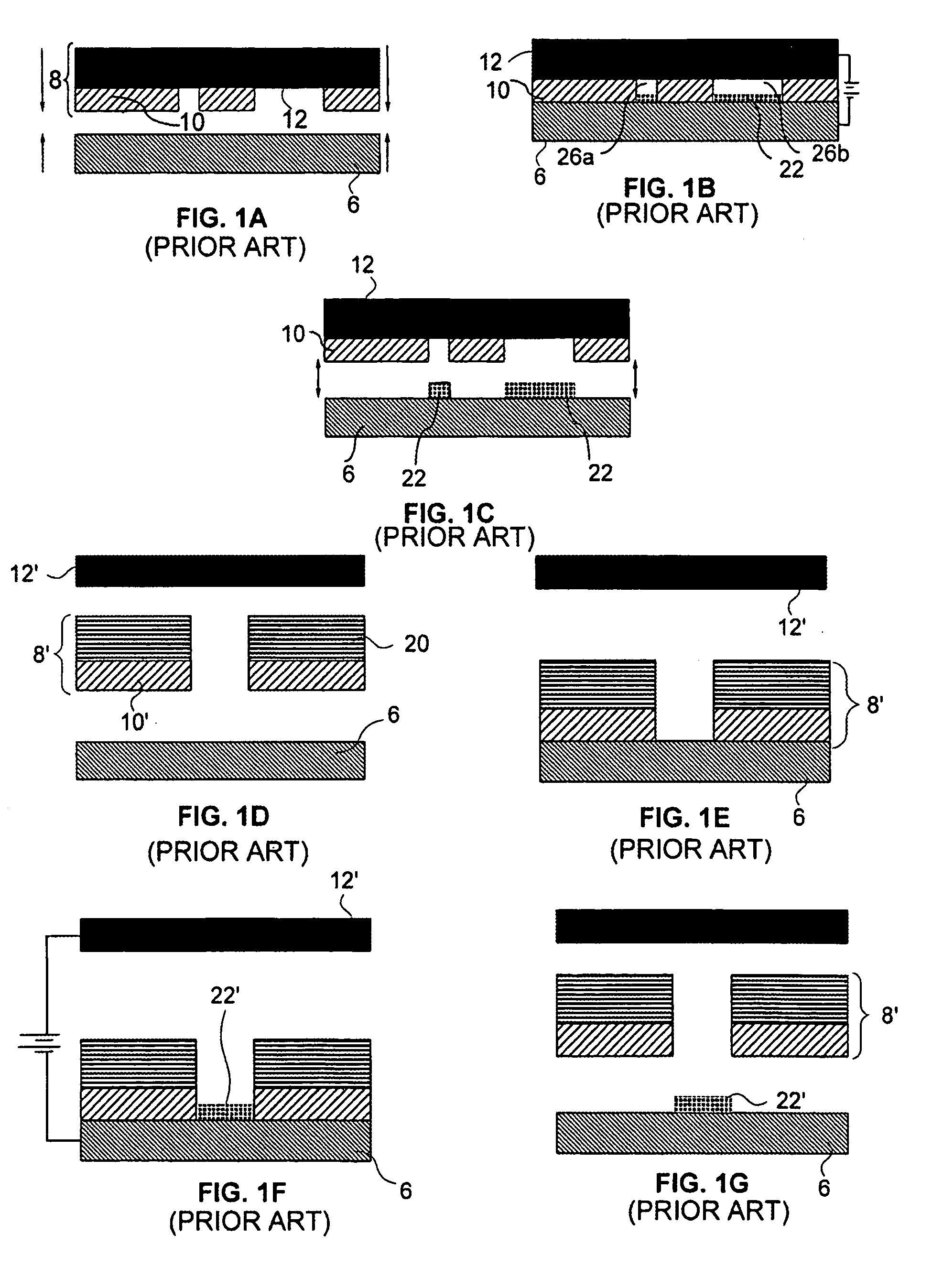
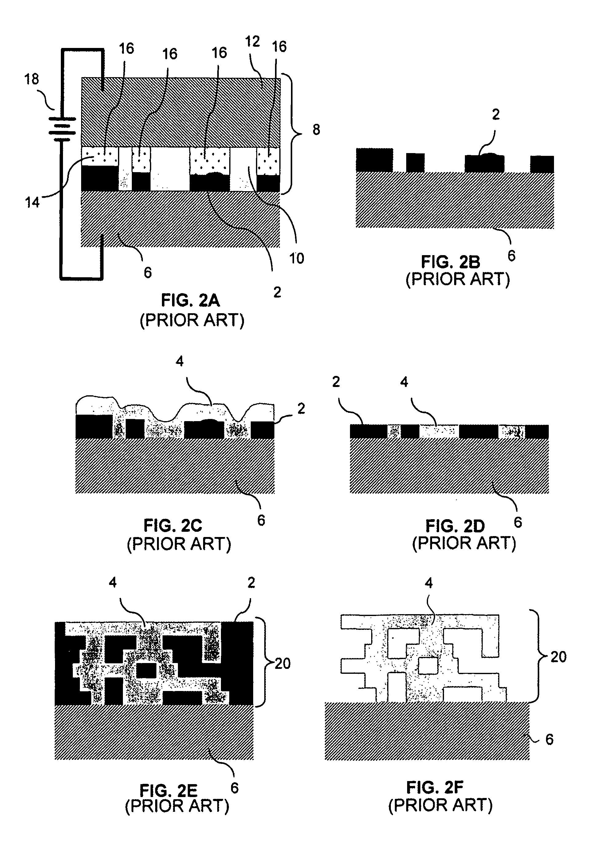
[0069]FIGS. 1(a)–1(g), 2(a)–2(f), and 3(a)–3(c) illustrate various features of one form of electrochemical fabrication that are known. Other electrochemical fabrication techniques are set forth in the '630 patent referenced above, in the various previously incorporated publications, in various other patents and patent applications incorporated herein by reference, still others may be derived from combinations of various approaches described in these publications, patents, and applications, or are otherwise known or ascertainable by those of skill in the art from the teachings set forth herein. All of these techniques may be combined with those of the various embodiments of the invention explicitly set forth herein to yield enhanced embodiments. Still other embodiments may be derived from combinations of the various embodiments explicitly set forth herein.

[0070]FIGS. 4(a)–4(i) illustrate various stages in the formation of a single layer of a multi-layer fabrication process where a se...


PUM

PropertyMeasurementUnit
three-dimensional structureaaaaaaaaaa
thicknessaaaaaaaaaa
conductiveaaaaaaaaaa

Abstract

A method of fabricating three-dimensional structures from a plurality of adhered layers of at least a first and a second material wherein the first material is a conductive material and wherein each of a plurality of layers includes treating a surface of a first material prior to deposition of the second material. The treatment of the surface of the first material either (1) decreases the susceptibility of deposition of the second material onto the surface of the first material or (2) eases or quickens the removal of any second material deposited on the treated surface of the first material. In some embodiments the treatment of the first surface includes forming a dielectric coating over the surface and the second material is electrodeposited (e.g. using an electroplating or electrophoretic process). In other embodiments the first material is coated with a conductive material that doesn't readily accept deposits of electroplated or electroless deposited materials.

Description

RELATED APPLICATIONS[0001]This application claims benefit of the following U.S. Provisional Patent Applications 60 / 468,979, filed May 7, 2003; 60 / 469,053, filed May 7, 2003; 60 / 533,891, filed Dec. 31, 2003; 60 / 468,977, filed May 7, 2003; and 60 / 534,204, filed Dec. 31, 2003. Each of these applications is hereby incorporated herein by references as if set forth in full herein.FIELD OF THE INVENTION[0002]Embodiments of various aspects of the invention relate to fabrication methods for forming three-dimensional structures (e.g. meso-scale or micro-scale structures) from layers that include at least two deposited materials wherein the methods include treating or deactivating a surface of a first deposited material such that deposition of a second material onto the surface of the first material is reduced or eliminated and wherein the surface may be activated, modified, or further treated to make it susceptible to receiving a subsequent deposition.BACKGROUND[0003]A technique for forming t...

Claims


Application Information

Patent Timeline
Patent Type & Authority Patents(United States)
IPC IPC(8): H01L21/311C23C18/16C25D5/02C25D5/10H01L21/44H01L21/768
CPCC25D5/022C25D5/10C23C18/1605H01L21/76879H01L21/7682B33Y10/00H01L21/288H01L21/311
Inventor COHEN, ADAM L.SMALLEY, DENNIS R.LOCKARD, MICHAEL S.LE, QUI T.
Owner MICROFAB
Why Eureka
Try Eureka