On-chip standalone self-test system and method

a self-testing and standalone technology, applied in the field of optical networking hardware testing, can solve problems such as defective transceiver chips

Inactive Publication Date: 2006-09-19
AVAGO TECH WIRELESS IP SINGAPORE PTE
View PDF28 Cites 40 Cited by
  • Summary
  • Abstract
  • Description
  • Claims
  • Application Information

AI Technical Summary

Benefits of technology

[0021]FIG. 3 is a more detailed block diagram of the single-chip multi-su...

Problems solved by technology

If the returned packets are inconsistent with th...

Method used


Image

  • On-chip standalone self-test system and method
  • On-chip standalone self-test system and method
  • On-chip standalone self-test system and method

Examples


Embodiment Construction

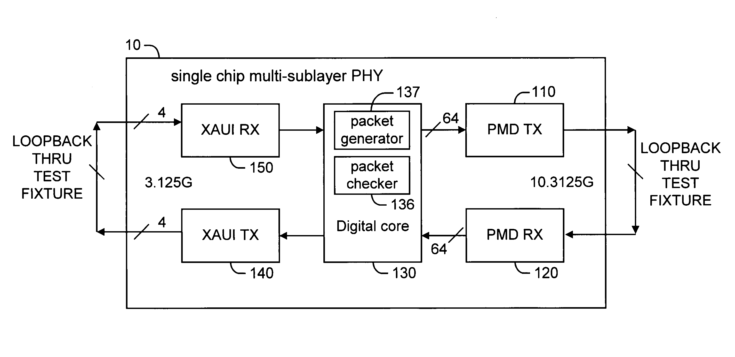
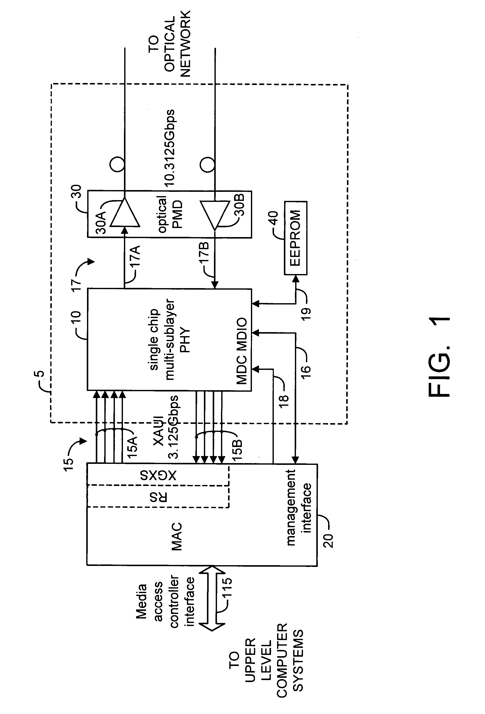
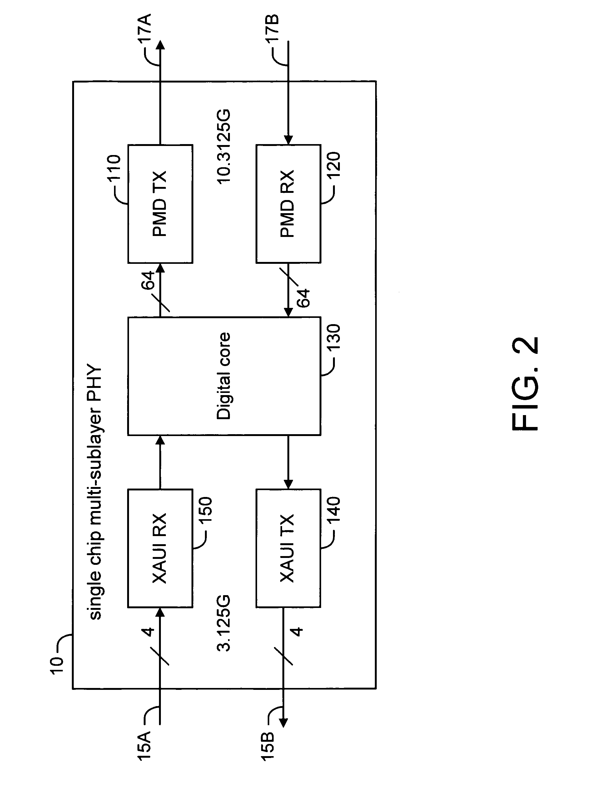
[0027]FIG. 1 is a schematic block diagram illustrating certain components of a 10 Gigabit transceiver module 5 with a XAUI (10 Gigabit attachment unit interface) 15 in accordance with an embodiment of the present invention. The transceiver module 5 may, in one embodiment of the present invention, be compatible with the XENPAK (XAUI module specification) optical module standard. The transceiver module 5 may, in another embodiment of the present invention, be compatible with the XPAK (second generation to XENPAK specification) optical module standard. The transceiver module 5 includes, for example, a single-chip multi-sublayer PHY (physical layer) 10 also known herein as the transceiver chip 10, an optical PMD (physical media dependent) 30, and an EEPROM 40.

[0028]According to an embodiment of the present invention, a media access controller (MAC) 20 interfaces to the single-chip multi-sublayer PHY 10 through the XAUI transmit and receive interface 15. In general, the MAC layer is one ...


PUM


Abstract

A method and system are disclosed for providing standalone built-in self-testing of a transceiver chip. The transceiver chip includes packet generators for generating test packets and packet checkers for comparing received packets with expected packets. The transceiver chip may be configured for testing through at least two wraparound test paths—a first test path that includes an elastic FIFO of a transmit path of the transceiver chip, and a second test path that includes an elastic FIFO of a receive path of the transceiver chip. During testing, the test packets are generated by packet generators within the transceiver chip and routed through the at least two wraparound test paths to packet checkers within the same transceiver chip. The packet checkers compare the returned packets to the expected packets. If the returned packets are inconsistent with the expected packets, the transceiver chip is defective.

Description

CROSS-REFERENCE TO RELATED APPLICATIONS / INCORPORATION BY REFERENCE[0001]U.S. Pat. No. 6,424,194, U.S. application Ser. No. 09 / 540,243 filed on Mar. 31, 2000, U.S. Pat. No. 6,389,092, U.S. Pat. No. 6,340,899, U.S. application Ser. No. 09 / 919,636 filed on Jul. 31, 2001, U.S. application Ser. No. 09 / 860,284 filed on May 18, 2001, U.S. application Ser. No. 10 / 028,806 filed on Oct. 25, 2001, U.S. application Ser. No. 09 / 969,837 filed on Oct. 1, 2001, U.S. application Ser. No. 10 / 159,788 entitled “Phase Adjustment in High Speed CDR Using Current DAC” filed on May 30, 2002, U.S. application Ser. No. 10 / 179,735 entitled “Universal Single-Ended Parallel Bus; fka, Using 1.8V Power Supply in 0.13 MM CMOS” filed on Jun. 21, 2002, U.S. application Ser. No. 60 / 401,872 entitled “SYSTEM AND METHOD FOR PERFORMING ON-CHIP SELF TESTING” filed on Aug. 7, 2002, and U.S. application Ser. No. 60 / 402,097 entitled “SYSTEM AND METHOD FOR IMPLEMENTING A SINGLE CHIP HAVING A MULTIPLE SUB-LAYER PHY” filed on Au...

Claims


Application Information

Patent Timeline
IPC IPC(8): G01R31/28H04B1/38H04L12/26H04B10/12H04L1/24
CPCH04L1/243
Inventor HOANG, TUAN M.JIANG, HONGTAO
Owner AVAGO TECH WIRELESS IP SINGAPORE PTE
Why Eureka
Try Eureka