Method of producing a contactless chip card or a contact/contactless hybrid chip card with improved flatness

a hybrid chip card and chip card technology, applied in the field of manufacturing a contact/contactless hybrid chip card with enhanced evenness, can solve the problems of over-the-counter methods with aesthetic disadvantages, darkening of colours, and manufacturing methods of contactless cards

Inactive Publication Date: 2006-10-03
ASK SA (FR)
View PDF15 Cites 18 Cited by
  • Summary
  • Abstract
  • Description
  • Claims
  • Application Information

AI Technical Summary

Benefits of technology

[0016]a first lamination step consisting in fusing onto each side of the antenna support two homogeneous sheets of thermoplastic by pressing at a temperature sufficient for the material of which the sheets are made to soften and flow wholly so as to eliminate any differences in thickness from the antenna support and to form a plasticised antenna support having even faces, and

Problems solved by technology

The above method unfortunately has an aesthetic disadvantage on the final presentation of the card.
Indeed, in the case of printed card bodies, during the lamination step of the card bodies onto the antenna support, the excessive thickness due to the antenna causes the impression points to be spaced apart resulting in brightening of the colour, and the cut-outs of the antenna support, into which the PVC of the inner layers of the card bodies flows, causes the impression points to be drawn closer together resulting in darkening of the colour.
This disadvantage also exists in the method of manufacturing contactless cards using a plastic antenna support onto which the antenna is produced by chemical etching.
Indeed, in such a method, after lamination, the imprint of the copper tracks is visible on the printed card bodies, and the unevenness of the card, even on a micron scale, can be seen by the user's eye as deformations of the graphics.

Method used


Image

  • Method of producing a contactless chip card or a contact/contactless hybrid chip card with improved flatness
  • Method of producing a contactless chip card or a contact/contactless hybrid chip card with improved flatness
  • Method of producing a contactless chip card or a contact/contactless hybrid chip card with improved flatness

Examples


Embodiment Construction

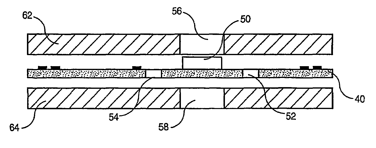
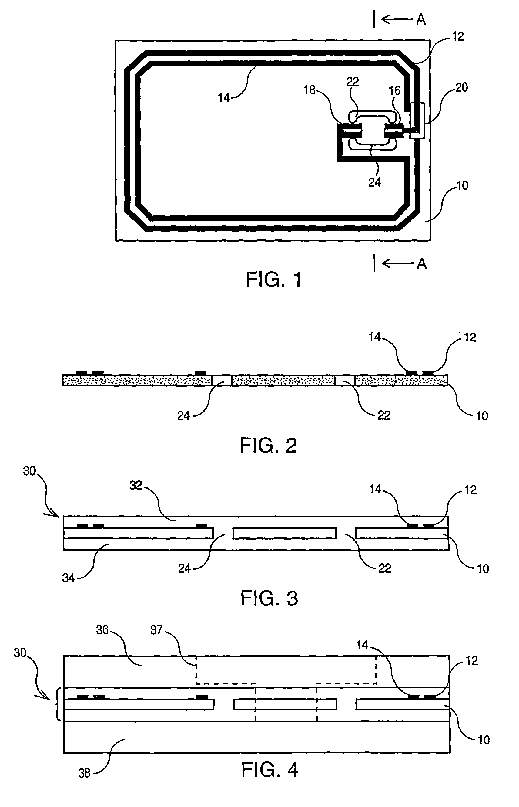
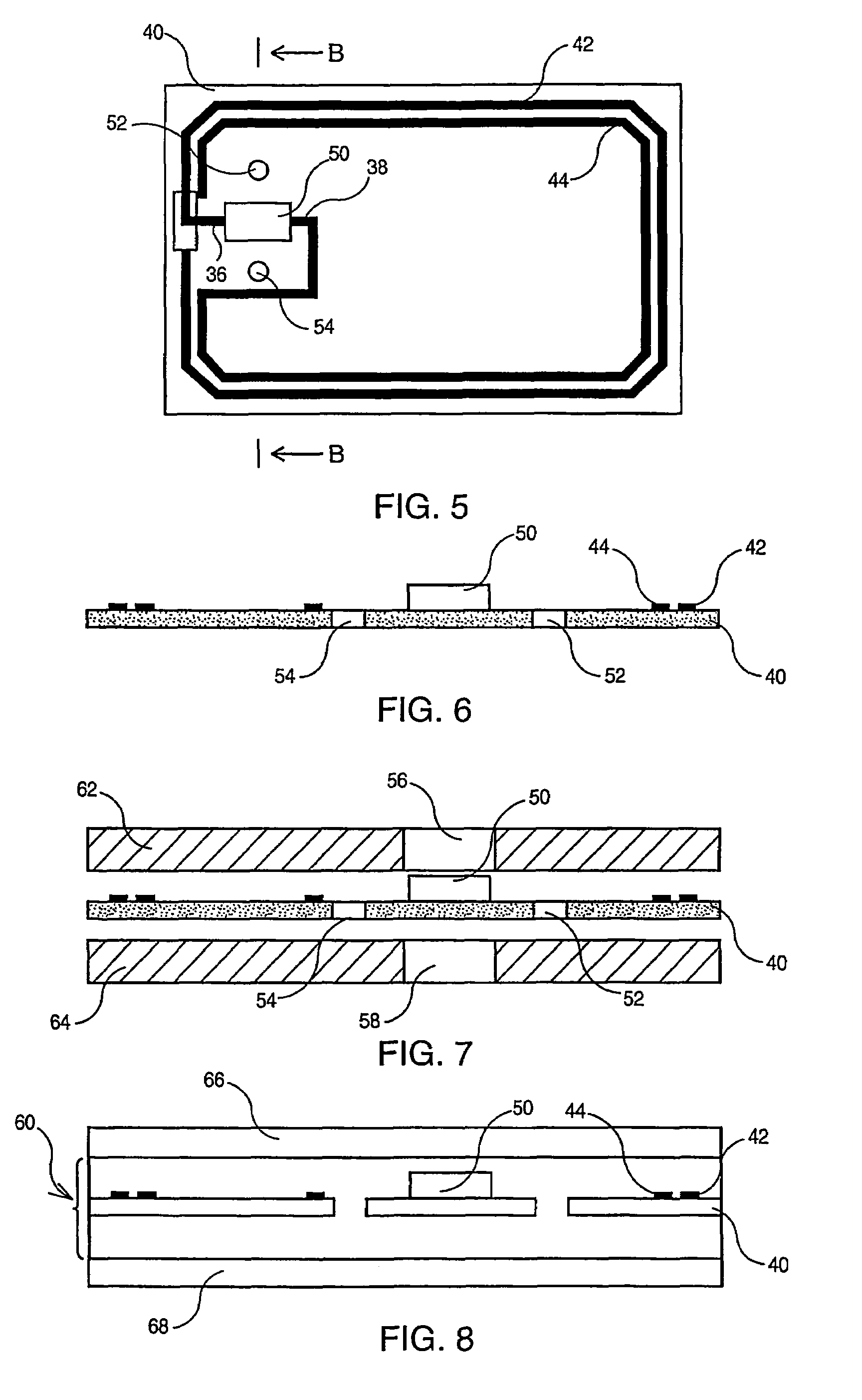
[0027]According to a preferred embodiment of the invention illustrated in FIG. 1, the antenna support is made of fibrous material such as paper and has a thickness of approximately 90 μm. The manufacture of the chip card according to the invention consists firstly in producing the antenna on its support 10. The antenna is made up of two loops 12 and 14 of screen-printed polymer conductor ink, containing conductive elements such as silver, copper or carbon. Each loop has one of its ends linked to one of the bonding pads of the antenna which are also screen-printed, loop 12 being linked to pad 16 and loop 14 to pad 18. The loops are interlinked by an electric bridge more commonly known as a cross-over (not shown in the figure) An insulating strip 20 of dielectric ink is screen-printed between the cross-over and loop 12. The electronic module containing the chip is inserted into the card at the last manufacturing step of the contact / contactless hybrid card. The antenna design is revers...


PUM

PropertyMeasurementUnit
temperaturesaaaaaaaaaa
temperatureaaaaaaaaaa
thicknessaaaaaaaaaa

Abstract

Method of manufacturing a chip card having an antenna support, two card bodies and an electronic module or a chip linked to the antenna. This method has a first lamination step which includes fusing two thermoplastic sheets (32, 34 or 62, 64) on each side of antenna support (10 or 40) at a temperature sufficient for the thermoplastic sheet material to soften and to flow wholly so as to eliminate any differences in thickness from the support, and a second lamination step carried out after a period of time necessary for the thermoplastic sheets (32, 34 or 62, 64) to be solidified, the second step including fusing by hot pressing two plastic layers (36, 38 or 66, 68) making up the card bodies onto the plasticised and even faces of uniformly thick antenna support (30 or 60) plasticised by the thermoplastic sheets.

Description

[0001]This application is a U.S. National Phase of International patent application PCT / FR03 / 002701, filed Sep. 12, 2003.TECHNICAL FIELD[0002]The present invention relates to the methods of manufacturing contact / contactless hybrid chip cards, and in particular to a method of manufacturing a contactless or contact / contactless hybrid chip card with enhanced evenness.BACKGROUNED ART[0003]The contactless chip card is a system used increasingly in various sectors. Thus, in the transport sector, it has been developed as a means of payment. This is also the case of electronic purses. Many companies have also developed means for identifying their personnel using contactless chip cards.[0004]The exchange of information between a contact / contactless hybrid card or a contactless card and the associated reading device is achieved by distance electromagnetic coupling between an antenna housed in the contactless card and a second antenna located in the reader or directly by contact with the reade...

Claims


Application Information

Patent Timeline
Patent Type & Authority Patents(United States)
IPC IPC(8): G08B13/14B42D15/10B32B37/00B32B37/02B32B37/20G06K19/07G06K19/077
CPCB32B37/02B32B37/04B32B37/203G06K19/07749B32B2305/342Y10T29/49002B32B2309/12B32B2425/00B32B2519/02B32B2309/02G06K19/077
Inventor KAYANAKIS, GEORGESBENATO, PIERREHALOPE, CHRISTOPHE
Owner ASK SA (FR)
Why Eureka
Try Eureka