Nonvolatile semiconductor memory device and method of programming in nonvolatile semiconductor memory device

a nonvolatile semiconductor and memory device technology, applied in the direction of digital storage, instruments, transistors, etc., can solve the problems of increasing the time required for programming, deteriorating reading accuracy, and increasing the number of programming operations, so as to improve the accuracy of read operations.

Active Publication Date: 2006-10-03
RENESAS ELECTRONICS CORP
View PDF3 Cites 29 Cited by
  • Summary
  • Abstract
  • Description
  • Claims
  • Application Information

AI Technical Summary

Benefits of technology

[0014]Therefore, an object of the present invention is to provide a nonvolatile semiconductor memory device and a method of programming thereof, which can make a width of threshold voltage distribution narrower.
[0015]Another object of the present invention is to provide a nonvolatile semiconductor memory device and a method of programming thereof, which can improve accuracy in a read operation.
[0017]According to the method mentioned above, a threshold voltage of a memory cell becomes higher than or equal to the first reference voltage in the first programming step. When the threshold voltage of the memory cell is lower than the second reference voltage that is higher than the first reference voltage, the threshold voltage is set to higher than or equal to the second reference voltage in the following second programming step. Here, the programming capability of the second program pulse applied to a control gate of the memory cell during the second programming step is lower than the programming capability of the final program pulse applied last in the first programming step. Therefore, a rate of increase in the threshold voltage in the second programming step is lower than a rate of increase in the threshold voltage in the first programming step. Thus, when the second reference voltage is set to a value slightly higher than the first reference voltage, the threshold voltage of the memory cell which is programmed in the second programming step does not exceed an upper bound of the threshold voltage distribution obtained due to the first programming step. In other words, the upper bound of the threshold voltage distribution obtained by the first programming step does not increase, while a lower bound of the threshold voltage distribution increases. Thus, a width of the threshold voltage distribution becomes narrower due to the second programming step, and hence a margin between two adjacent distributions becomes wider. Therefore, the accuracy in a read operation is improved.
[0028]According to the nonvolatile semiconductor memory device and the method of programming, The programming capability of the second program pulse applied in the second programming mode (step) is lower than the programming capability of the final program pulse applied last in the first programming mode (step). Therefore, a rate of increase in the threshold voltage in the second programming step is lower than a rate of increase in the threshold voltage in the first programming step. Thus, the threshold voltage of the memory cell which is programmed in the second programming step does not exceed an upper bound of the threshold voltage distribution obtained due to the first programming step. In other words, the upper bound of the threshold voltage distribution obtained by the first programming step does not increase, while a lower bound of the threshold voltage distribution increases. Thus, a width of the threshold voltage distribution becomes narrower due to the second programming step, and hence a margin between two adjacent distributions becomes wider. Therefore, the accuracy in a read operation is improved.

Problems solved by technology

The narrower margin can cause a read error and hence deterioration of reading accuracy.
In this case, however, there are problems in that the number of programming operations increases and hence the time necessary for the programming increases.
However, the reference value Vref can fluctuate due to influences of noises.
Such a problem can also occur in the case of the above-mentioned Patent Document No. 1.

Method used


Image

  • Nonvolatile semiconductor memory device and method of programming in nonvolatile semiconductor memory device
  • Nonvolatile semiconductor memory device and method of programming in nonvolatile semiconductor memory device
  • Nonvolatile semiconductor memory device and method of programming in nonvolatile semiconductor memory device

Examples


Embodiment Construction

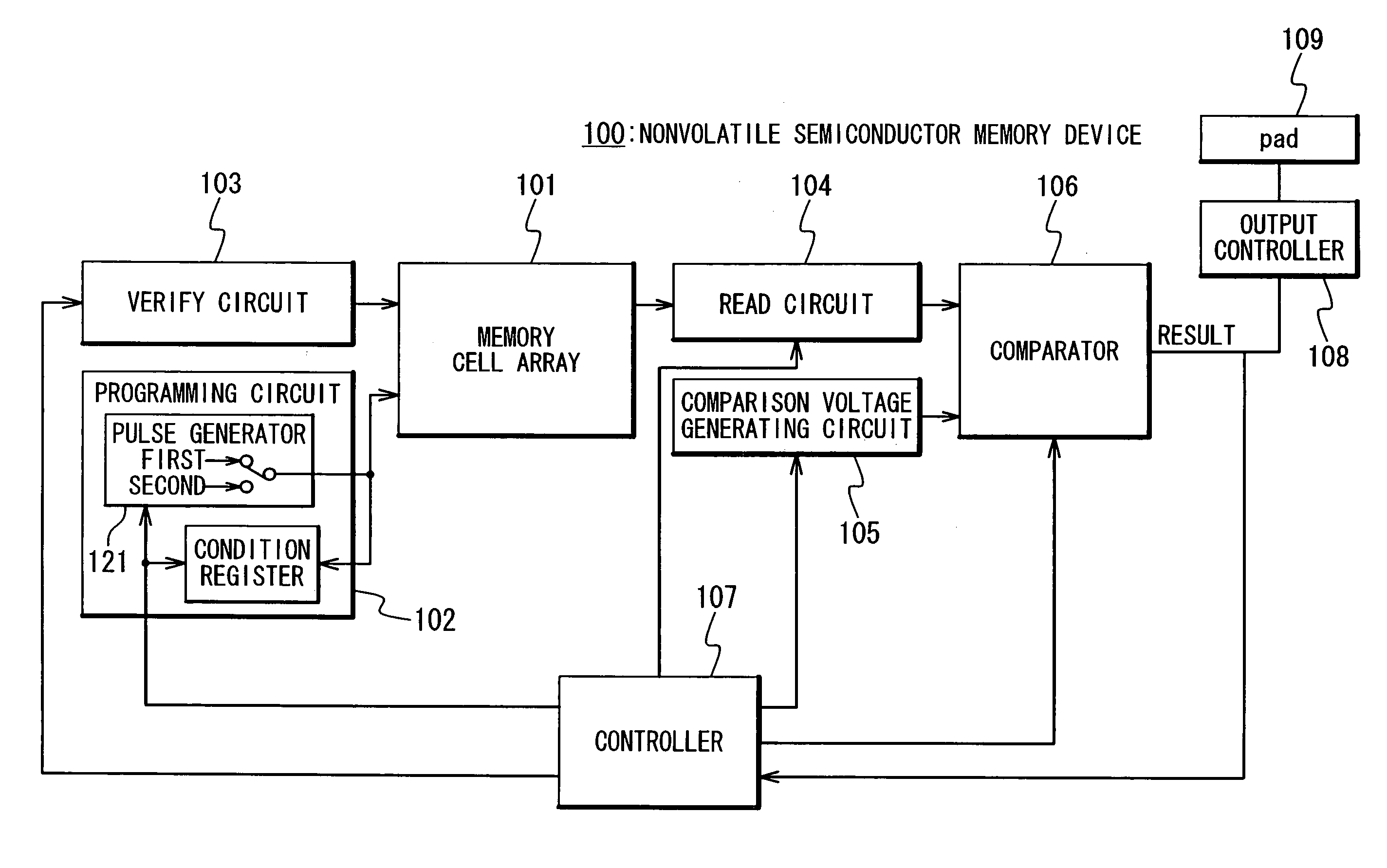
[0039]Embodiments of the present invention will be described below with reference to the attached drawings. FIG. 6 shows a nonvolatile semiconductor memory device 100 including a programming device according to an embodiment of the present invention. The nonvolatile semiconductor memory device 100 has a memory cell array 101, a programming circuit 102 (writing circuit), a verify circuit 103, a read circuit 104, a comparison voltage generating circuit 105, a comparator 106, and a controller 107. The programming circuit 102, the verify circuit 103, the read circuit 104, the comparison voltage generating circuit 105, the comparator 106, and the controller 107 configure the programming device.

[0040]The memory cell array 101, which is the target of the programming, is configured as a flash memory cell array. The memory cell array 101 includes a plurality of memory cells which are arrayed in a matrix form. Each of the memory cells has a stacked gate structure (floating gate structure). Th...


PUM


Abstract

A memory cell array includes a plurality of memory cells each of which has a control gate and a floating gate. A programming circuit operates in a first programming mode followed by a second programming mode. In the first programming mode, the programming circuit applies a first program pulse to first memory cells while progressively increasing a programming capability of the first program pulse until threshold voltages of the first memory cells become higher than or equal to a first reference voltage. In the second programming mode, the programming circuit applies a second program pulse to second memory cells included in the first memory cells and having threshold voltages lower than a second reference voltage that is higher than the first reference voltage until the threshold voltages of the second memory cells become higher than or equal to the second reference voltage.

Description

BACKGROUND OF THE INVENTION[0001]1. Field of the Invention[0002]The present invention relates to a nonvolatile semiconductor memory device and a method of programming in the nonvolatile semiconductor memory device. More specifically, the present invention relates to a nonvolatile semiconductor memory device having a plurality of memory cells each of which can store a multi-level data, and a method of programming in the nonvolatile semiconductor memory device.[0003]2. Description of the Related Art[0004]Generally speaking, a nonvolatile semiconductor memory device such as a flash memory includes a plurality of memory cells each of which has a stacked gate structure (floating gate structure). That is to say, in a MOS transistor of the memory cell, a floating gate is provided between a substrate and a control gate. When charges are injected into the floating gate, a threshold value (threshold voltage) of each memory cell varies in accordance with the amount of the injected charges. In ...

Claims


Application Information

Patent Timeline
Patent Type & Authority Patents(United States)
IPC IPC(8): G11C16/04G11C16/02G11C11/34G11C16/06G11C16/10G11C16/12G11C16/34H01L21/8247H01L27/115H01L29/788H01L29/792
CPCG11C16/12G11C16/3468
Inventor SUZUKI, JUNICHIKANAMORI, KOHJI
Owner RENESAS ELECTRONICS CORP
Why Eureka
Try Eureka