Apparatus and method for realizing all-optical NOR logic device using gain saturation characteristics of a semiconductor optical amplifier

a technology of alloptical nor logic devices, applied in the direction of semiconductor lasers, pulse techniques, instruments, etc., can solve the problems of difficult integration of complicated optical fiber devices with other devices, uncertain future reliability, and inability to meet the requirements of optical operating systems which require a high degree of integration

Inactive Publication Date: 2006-10-17
KOREA INST OF SCI & TECH
View PDF34 Cites 10 Cited by
  • Summary
  • Abstract
  • Description
  • Claims
  • Application Information

AI Technical Summary

Problems solved by technology

For this reason, their future reliability is somewhat uncertain since they are expected to face a serious limitation in terms of their speed and the quantity of information that can be processed.
However, it is unsuitable for an application in optical operating systems which require a high degree of integration.
Also, their essential components consist of complicated optical fiber devices whose integration with other devices are also difficult.

Method used


Image

  • Apparatus and method for realizing all-optical NOR logic device using gain saturation characteristics of a semiconductor optical amplifier
  • Apparatus and method for realizing all-optical NOR logic device using gain saturation characteristics of a semiconductor optical amplifier
  • Apparatus and method for realizing all-optical NOR logic device using gain saturation characteristics of a semiconductor optical amplifier

Examples


Embodiment Construction

[0043]Hereinafter, preferred embodiments of the present invention will be described in detail with reference to the accompanying drawings.

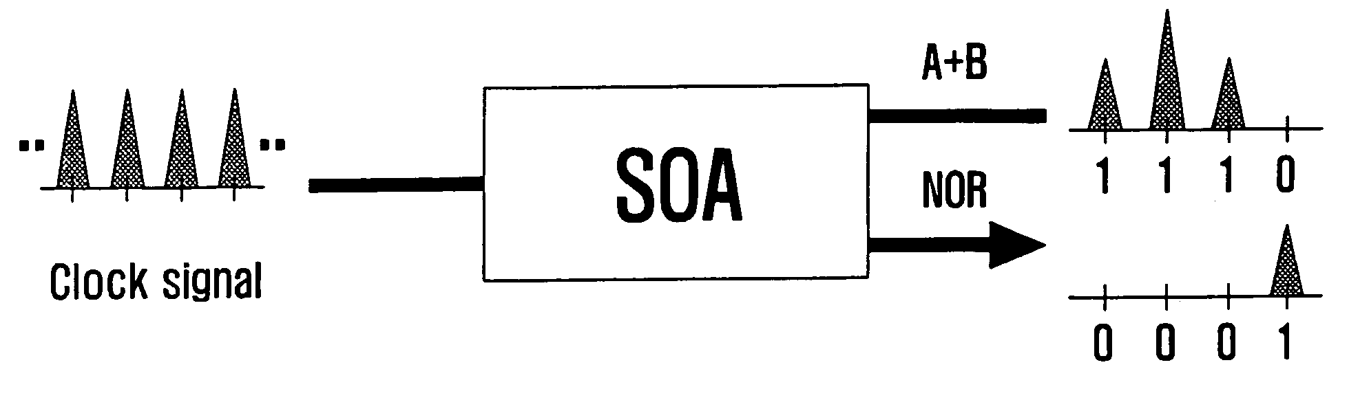
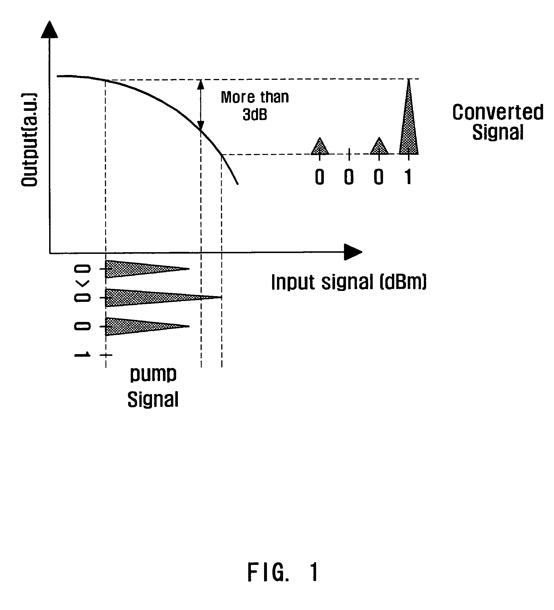
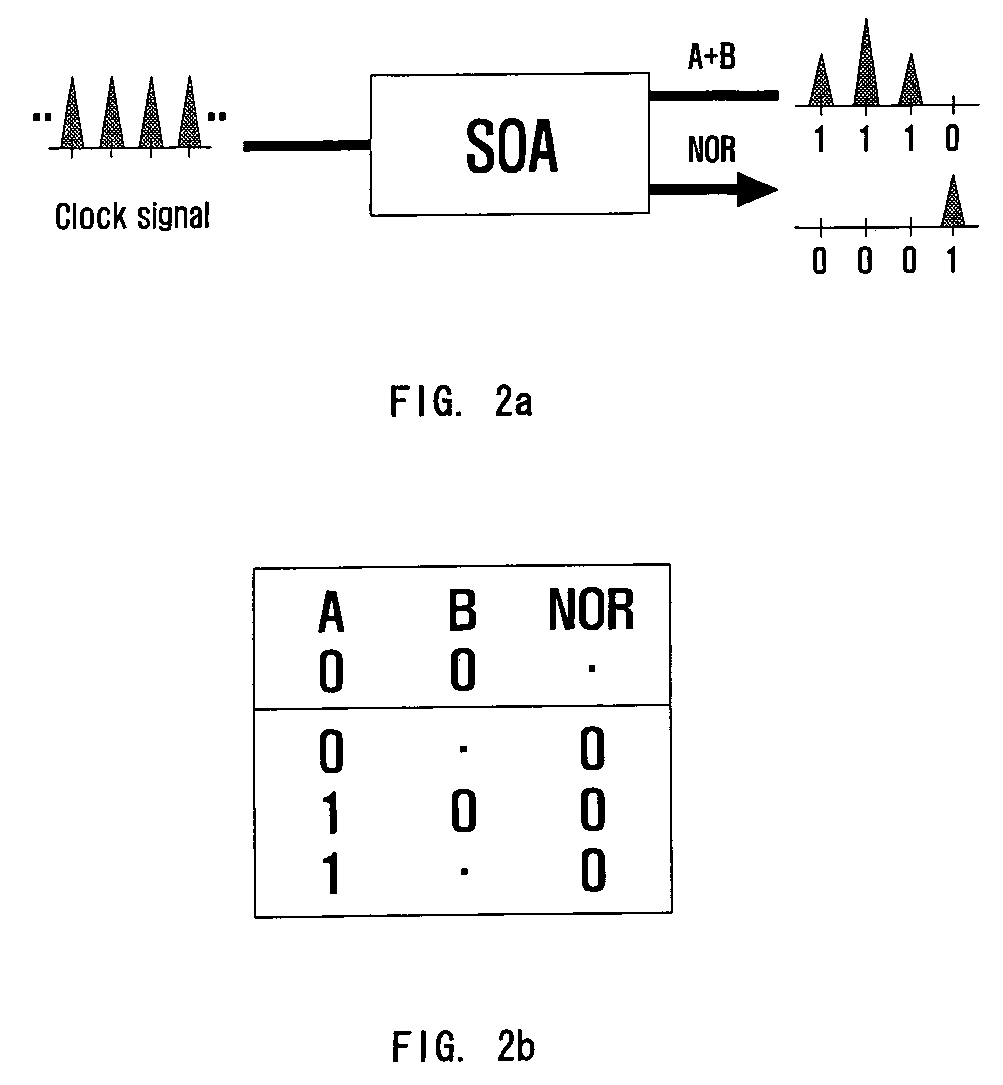
[0044]FIG. 1 is a conceptual diagram which shows the operational principle of an all-optical NOR logic device.

[0045]According to the present invention, the probe signal and pump signal are generated in return-to-zero (RZ) pattern signals in order to improve the operating speed.

[0046]If a pump signal with a high power is coupled into a semiconductor optical amplifier (SOA), carrier depletion occurs in the SOA.

[0047]Accordingly, since a probe signal in a pulse form with a fixed period is outputted after identically modulated to the gain modulation through carrier depletion within the SOA, the output signal has an opposite logic to the pump signal.

[0048]However, since the On-Off difference of the pulses is large when the pulse signal is used, the size of the output signal when the pulse signal is not present is small enough to be considered as 0.

[004...


PUM

PropertyMeasurementUnit
wavelengthaaaaaaaaaa
time delayaaaaaaaaaa

Abstract

The present invention relates to an apparatus and a method for realizing all-optical NOR logic device using the gain saturation characteristics of a semiconductor optical amplifier(SOA). More particularly, the invention relates to a 10 Gbit / s all-optical NOR logic device among all-optical logic devices, in which a signal transmitted from a given point of an optical circuit such as an optical computing circuit is used as a pump signal and a probe signal.The method for realizing an all-optical NOR logic device using the gain saturation characteristics of the SOA according to the present invention comprises the steps of: utilizing A+B signal which couples together an input signal pattern A (1100) and an input signal pattern B (0110) as a pump signal (1110); utilizing a probe signal (1111) by generating a clock signal out of said input signal pattern A (1100); and obtaining a Boolean equation {overscore (A+B)} by making said probe signal and said pump signal incident upon the SOA simultaneously from the opposite direction.The all-optical logic device according to the present invention has a simple construction since it is realized through the XGM (Cross Gain Modulation) method which utilizes the gain saturation characteristics. Also, it is expected that the method employed in the present invention could be used for realizing other all-optical logic circuits and devices.

Description

BACKGROUND OF THE INVENTION[0001]The present invention relates to an apparatus and a method for realizing an all-optical NOR logic device using the gain saturation characteristics of a semiconductor optical amplifier SOA. More particularly, the invention relates to a 10 Gbit / s all-optical NOR logic device among all-optical logic devices, in which a signal transmitted from a given point of an optical circuit such as an optical computing circuit is used as a pump signal and a probe signal.[0002]The recent trends show that the requirement for a high capacity and a high speed system is exponentially increasing.[0003]Most of the present systems are based on silicon materials which operate on the basis of electric signals. For this reason, their future reliability is somewhat uncertain since they are expected to face a serious limitation in terms of their speed and the quantity of information that can be processed.[0004]On the contrary, the systems utilizing the optical devices which are ...

Claims


Application Information

Patent Timeline
Patent Type & Authority Patents(United States)
IPC IPC(8): G02F3/00
CPCG02F3/00H01S5/50G02F1/3515G02F2203/70H01S5/509
Inventor BYUN, YOUNG TAEKIM, JAE HUNJHON, YOUNG MINLEE, SEOKWOO, DEOK HAKIM, SUN HOYI, JONG CHANG
Owner KOREA INST OF SCI & TECH
Why Eureka
Try Eureka