Optical signal amplification device

a technology of optical signal and amplifier, which is applied in the direction of semiconductor amplifier structure, semiconductor laser, instruments, etc., can solve the problems of spontaneous emission of light, and achieve the effect of high flexibility in various kinds of optical circuits, compact size or integrated into a single chip

Inactive Publication Date: 2006-10-31
OPTOTRIODE
View PDF13 Cites 2 Cited by
  • Summary
  • Abstract
  • Description
  • Claims
  • Application Information

AI Technical Summary

Benefits of technology

[0013]The gist of a fourth invention is that, in the above-described second invention, the optical signal amplification device is equipped with second input-light inputting means for inputting a second input light which has a wavelength that is different from the first wavelength, to the second optical amplifying element, for enhancing the negative feedback amplification effect of the first optical amplifying element.
[0031]The gist of an eleventh invention is that the optical signal amplification device constitutes a part or all of an optical operational amplifier, an optical differential amplification circuit, an optical adding / subtracting circuit, an optical differentiating / integrating circuit, an optical flip-flop circuit, an optical limiter and a light surge suppressor. The optical signal amplification device of the eleventh invention provides a high flexibility in various kinds of optical circuits.

Problems solved by technology

That is, it is common that the spontaneous emission light as the surrounding light is removed by a filter, since it becomes a factor of noise generation.

Method used


Image

  • Optical signal amplification device
  • Optical signal amplification device
  • Optical signal amplification device

Examples


embodiment 1

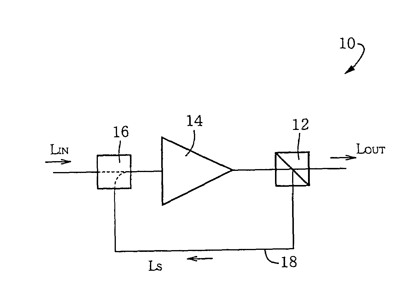
[0056]Referring to the drawings, there will be described in detail an optical signal amplification device 10 of one embodiment of the present invention which is equipped with a negative feedback amplification function.

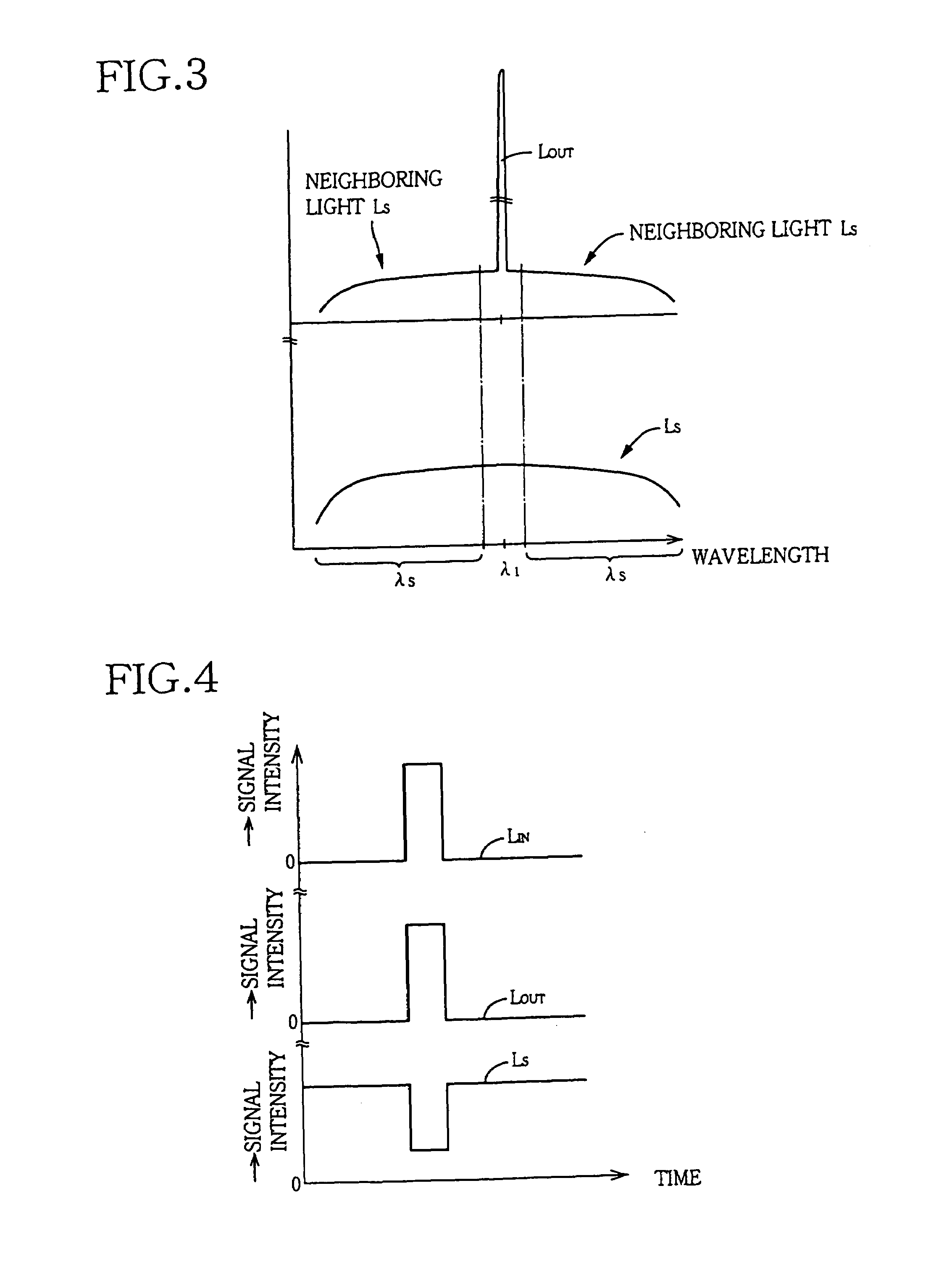
[0057]In FIG. 1, there is shown a wavelength selecting element 12, which is provided to extract, from an output light outputted from a first optical amplifying element 14, an output signal light LOUT of a first wavelength λ1 of, for example, 1550 nm and a neighboring light LS having a wavelength other than the first wavelength λ1. That is, the wavelength selecting element 12 renders the light having a predetermined wavelength of 1545–1555 nm (whose central value is 1550 nm) to be transmitted therethrough, while reflecting all or a part of the light having a wavelength λS (i.e., a predetermined wavelength band corresponding to a range of λSS>1555 nm) that is other than the above-described predetermined wavelength. This wavelength selecting element 12 may be constituted ...

embodiment 2

[0063]Next, there will be described other embodiments of the present invention. In the following embodiments, the same reference signs as used in the above-described embodiment will be used to identify the common parts, and description of these parts will not be provided.

[0064]FIG. 5 shows a monolithic arrangement as another example in which the above-described optical signal amplification device 10 is mounted on a single semiconductor chip. In FIG. 5, on a semiconductor substrate 28a, there is formed a waveguide 28b, which consists of a straight portion and an elliptic portion that overlaps with a central part of the straight portion so as to be connected with the straight portion. An upper electrode 28c is provided in a portion of the waveguide 28b, which portion corresponds to the central part of the straight portion and a part of the elliptic portion, so as to function as the above-described first optical amplifying element 14. A wavelength selecting element 30, having a refract...

embodiment 3

[0065]FIG. 6 is a view explaining the construction of an optical signal amplification device 42 of another embodiment of the present invention. In FIG. 6, the neighboring light LS, which has been separated by the wavelength selecting element 12, is inputted to a second optical amplifying element 44 via the optical feedback path 18. The neighboring light LS is amplified in the second optical amplifying element 44, and is then coupled with the input signal light LIN in an optical coupler 46, so that the neighboring light LS, together with the input signal light LIN, is inputted to the first optical amplifying element 14. Unlike the wavelength selecting element 12, the optical coupler 46 does not have to be provided by a filter, as long as it is capable of coupling the output light of the second optical amplifying element 44 and the input signal light LIN with each other. However, the optical coupler 46 may be provided by the above-described optical add / drop filter or the like. As desc...


PUM


Abstract

An optical signal amplification device for outputting an output signal light which has the same wavelength as an input signal light and an intensity variation identical in phase with an intensity variation of the input signal light. The device includes: (a) an amplifying element having a cross gain modulation function of outputting an output light including (i) the output signal light and (ii) a neighboring light which has a neighboring wavelength different from the wavelength of the output signal light and an intensity variation inverted in phase with respect to the intensity variation of the output signal light; (b) inputting means for inputting the input signal light to the amplifying element; (c) a selecting element extracting the output signal light and at least a part of the neighboring light from the output light, such that the extracted output signal light and neighboring light are separated from each other; and (d) feedback means for feeding back the neighboring light extracted by the selecting element, to the amplifying element, so that the neighboring light is inputted to the amplifying element, for rendering the amplifying element to generate a negative feedback amplification effect.

Description

TECHNICAL FIELD[0001]The present invention relates to an optical signal amplification device suitable for optoelectronics such as optical communication, optical image processing, optical computation and optical measurement, which require advanced optical signal processing.BACKGROUND ART[0002]Conventionally, an erbium-doped fiber amplifier (EDFA) and a semiconductor optical amplifier (SOA) are used for amplifying a light signal. Actually, however, for eliminating noise generated in such an amplifier, the light signal that is transmitted at a high speed is once converted into an electrical signal, so as to be subjected to noise elimination and signal processing in an electronic circuitry, and the processed signal is then reconverted into a light signal to be transmitted. This incapability to achieve direct processing of a light signal without its conversion into an electrical signal limits the speed of the optical signal processing.[0003]Therefore, in broad-band information services s...

Claims


Application Information

Patent Timeline
Patent Type & Authority Patents(United States)
IPC IPC(8): H01S3/00H01S5/00H04B10/12H01S5/50
CPCG02F2/004H01S3/1302H01S3/1305H01S3/2333H01S5/0078H01S5/50H01S5/5072H04B10/291H04B10/296H01S5/02325
Inventor MAEDA, YOSHINOBU
Owner OPTOTRIODE
Why Eureka
Try Eureka