Method of fabricating flash memory device

a flash memory and device technology, applied in the direction of fixed installation, lighting and heating apparatus, rod connection, etc., can solve the problems of inability to further adopt the self-aligned shallow trench isolation method (sti) and the gap-filling method using high density plasma (hdp) oxide film, and achieve the effect of improving the trench-filling characteristics and reducing the thickness of sidewall oxide film

Inactive Publication Date: 2006-10-24
SK HYNIX INC
View PDF1 Cites 5 Cited by
  • Summary
  • Abstract
  • Description
  • Claims
  • Application Information

AI Technical Summary

Benefits of technology

[0007]The patent also discloses a method of fabricating a flash memory device, wherein trench gap-fill characteristics can be improved.
[0008]To accomplish this, there is provided a method of fabricating a flash memory device, including the steps of forming a screen oxide film and a pad nitride film on a semiconductor substrate, etching the pad nitride film, the screen oxide film and the semiconductor substrate to form trenches, forming sidewall oxide films on the surface of the semiconductor substrate in which the trenches are formed, and regrowing the screen oxide film in such a way to have a predetermined thickness, reducing a thickness of the sidewall oxide films, forming a liner nitride film on the entire surface including the trenches, forming element isolation films within the trenches, removing the liner nitride film and the pad nitride film to expose the element isolation films that are projected upwardly from the semiconductor substrate, etching the entire surface so that the screen oxide film is removed, thereby reducing the width of the element isolation films, which are exposed due to the removal of the pad nitride film, and forming floating gates with tunnel dielectric films being intervened between neighboring element isolation films.

Problems solved by technology

As a flash memory device is highly integrated, lots of difficulties are encountered in constructing an element isolation film of the flash memory device.
The most important problem is that the element isolation film is gap-filled into a trench having a narrow width and a deep depth, of a high aspect ratio.
As the flash memory device is highly integrated below 70 nm, an existing self-aligned shallow trench isolation (STI) method and gap-filling using a high density plasma (HDP) oxide film cannot be further adopted due to the lack of margin.
It reaches a point where securing the space between floating gates becomes impossible through simple mask and etch work.
Even if the SAFG technology has been introduced, however, there inevitably occurs a trench burial problem.

Method used


Image

  • Method of fabricating flash memory device
  • Method of fabricating flash memory device
  • Method of fabricating flash memory device

Examples


Embodiment Construction

[0031]Various embodiments will be described with reference to the accompanying drawings. Those of ordinary skill in the art will appreciate that the disclosed embodiments may be modified in various manners and the scope of the present patent is not limited by the embodiments described later.

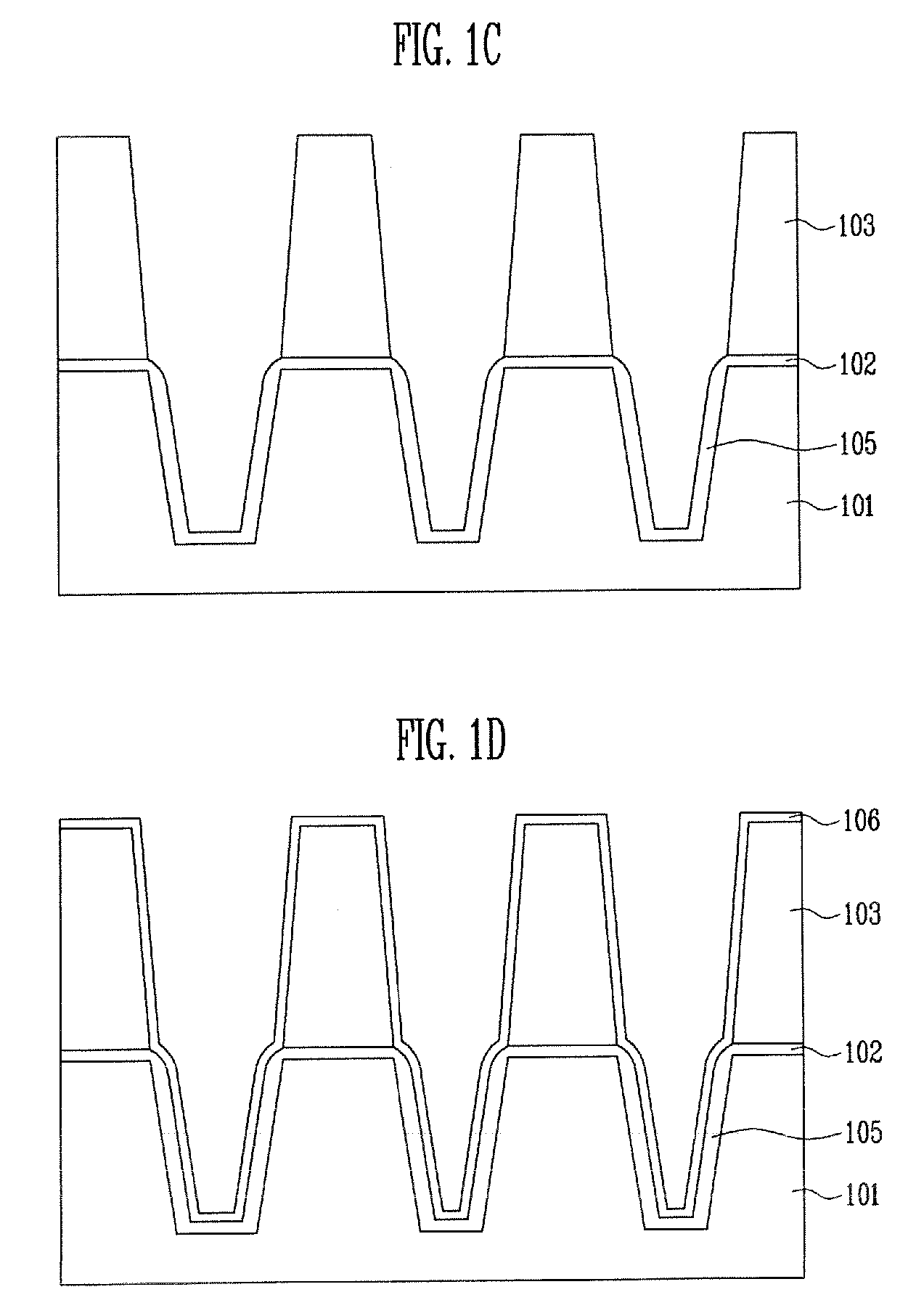
[0032]FIGS. 1a to 1i are cross-sectional views illustrating process steps in an exemplary method of fabricating a flash memory device.

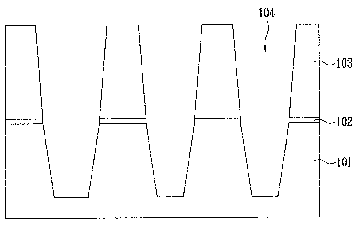
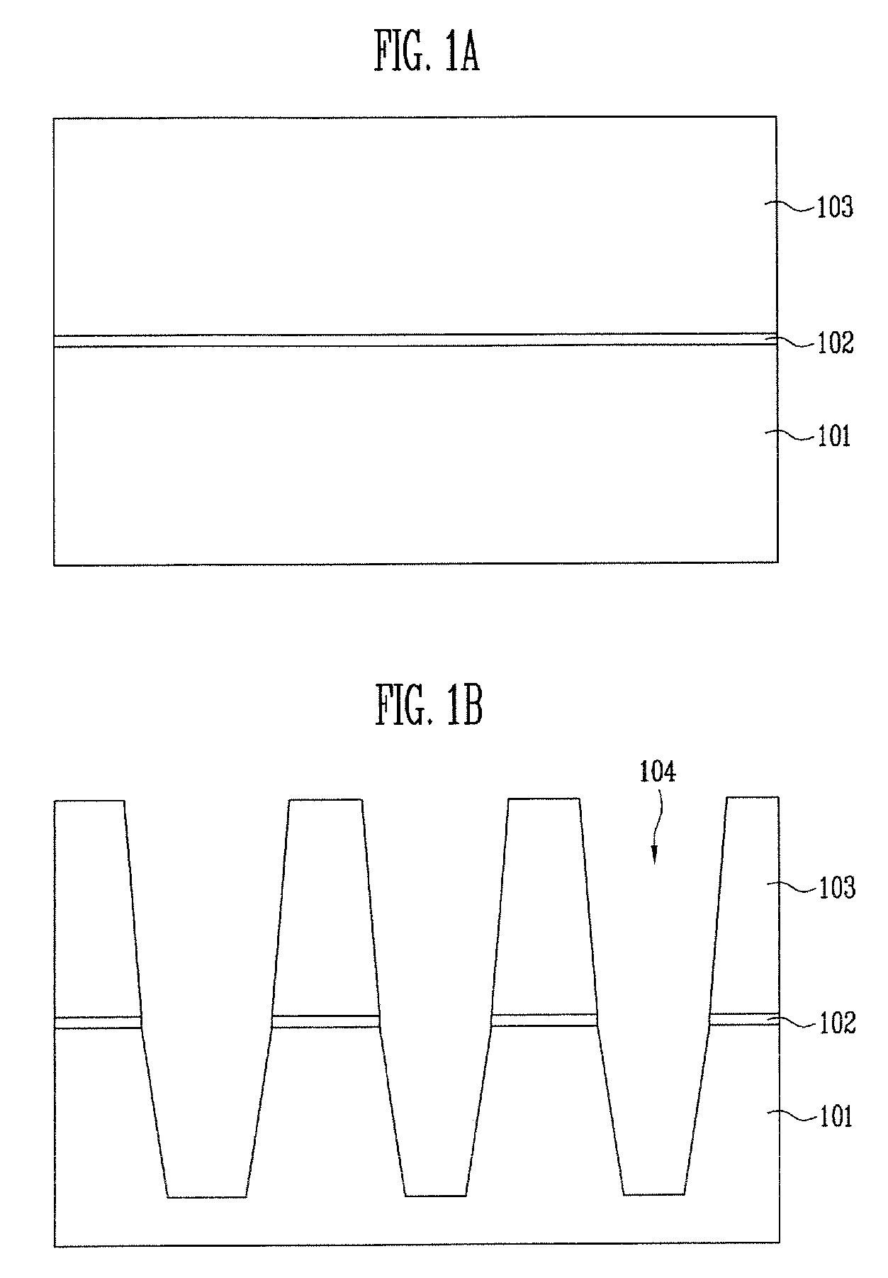
[0033]Referring to FIG. 1a, a screen oxide film 102 is formed on a semiconductor substrate 101. After a well ion and various threshold voltage (Vt) ions are implanted, a pad nitride film 103 is deposited on a screen oxide film 102 in order to pattern an element isolation film.

[0034]In this case, the screen oxide film 102 is formed to a thickness of approximately 20 to 50 Å. The pad nitride film 103 is formed to a thickness sufficient enough to secure the height of a floating gate at the time of chemical mechanical polishing (hereinafter, referred to as “CMP”) among...


PUM


Abstract

A method of fabricating a flash memory devices disclosed wherein, upon formation of sidewall oxide films, a regrown thickness of a screen oxide film is controlled. The width of an element isolation film is reduced by means of an etch process for removing the re-growth oxide film. This allows a floating gate space to be easily secured, and a thickness of the sidewall oxide films is reduced by means of a liner nitride film pre-treatment cleaning process. It is thus possible to secure the trench space, which facilitates gap-filling.

Description

CROSS REFERENCE TO RELATED APPLICATIONS[0001]This application relies for priority upon Korean Patent Application No. 2005-20218 filed on Mar. 10, 2005, the contents of which are herein incorporated by reference in their entirety.FIELD OF THE INVENTION[0002]The present patent relates to a method of fabricating a flash memory device, and more specifically, to a method of fabricating a flash memory device, wherein gap-fill characteristics of an element isolation film of a high integrated flash memory device can be improved.DISCUSSION OF RELATED ART[0003]As a flash memory device is highly integrated, lots of difficulties are encountered in constructing an element isolation film of the flash memory device. The most important problem is that the element isolation film is gap-filled into a trench having a narrow width and a deep depth, of a high aspect ratio.[0004]As the flash memory device is highly integrated below 70 nm, an existing self-aligned shallow trench isolation (STI) method and...

Claims


Application Information

Patent Timeline
Patent Type & Authority Patents(United States)
IPC IPC(8): H01L21/336
CPCH01L21/76232H01L27/115H01L27/11521H10B69/00H10B41/30E04H12/085F16B7/182F16B7/187F21S8/085
Inventor DONG, CHA DEOK
Owner SK HYNIX INC
Why Eureka
Try Eureka