

Lower power high speed design in BiCMOS processes
a high-speed design, low-power technology, applied in logic circuits, logic circuits, logic circuits characterised by logic functions, etc., can solve the problems of power and maximum frequency trade-off, lower frequency capability, and voltages that cannot be operated at 1.8v
- Summary
- Abstract
- Description
- Claims
- Application Information
AI Technical Summary
Benefits of technology
Problems solved by technology
Method used
Image

Examples
Embodiment Construction
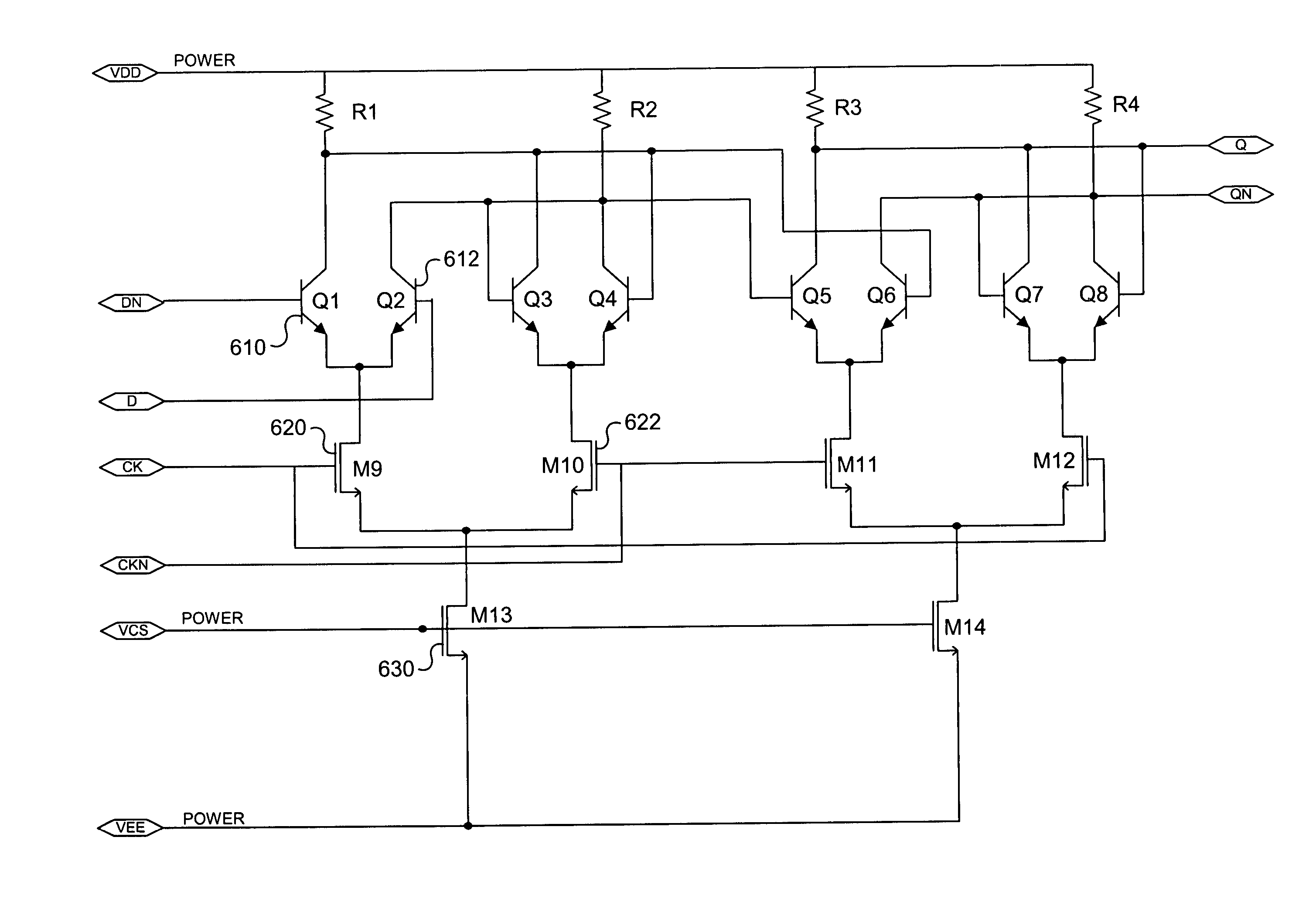
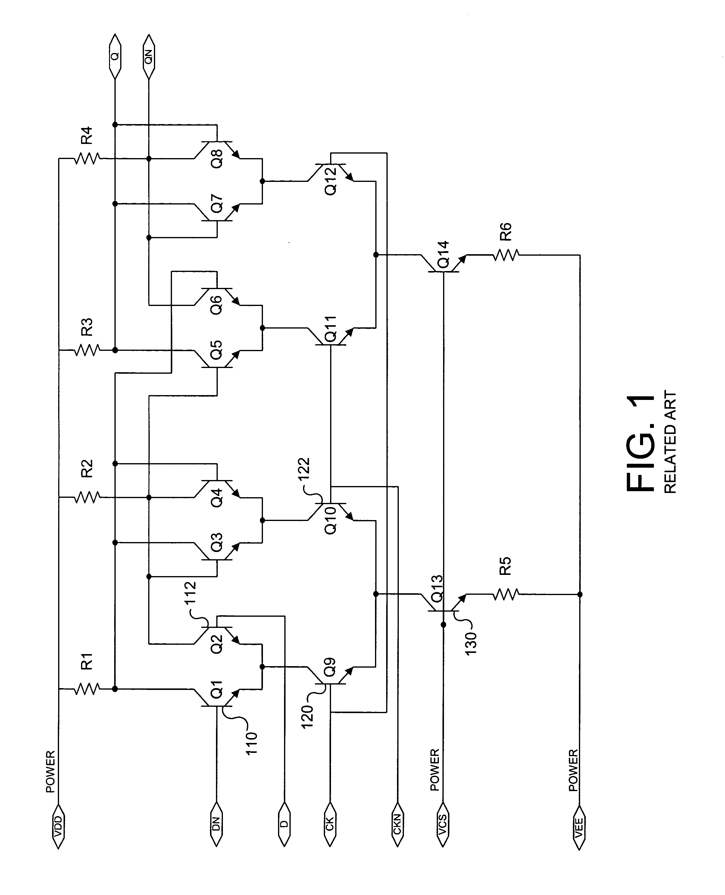
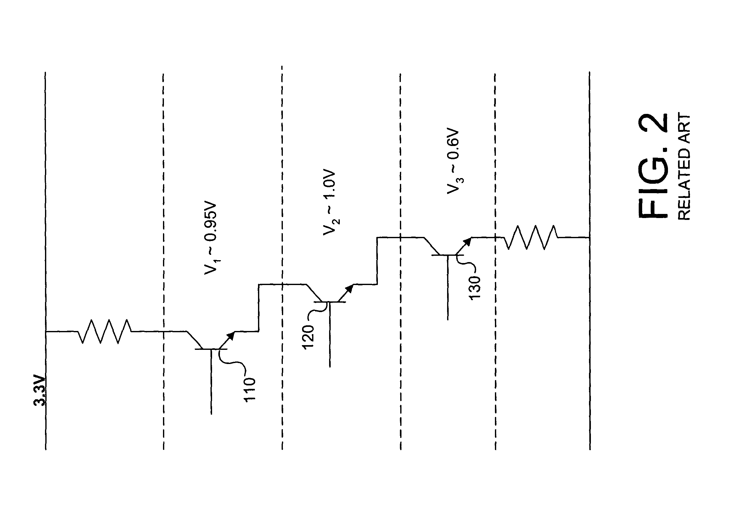
[0027]In the following detailed description of preferred embodiments, reference is made to the accompanying drawings that show, by way of illustration, specific embodiments in which the invention may be practiced. In the drawings, like numerals describe substantially similar components throughout the several views. These embodiments are described in sufficient detail to enable those skilled in the art to practice the invention. Other embodiments may be utilized, and structural, logical, and intellectual changes may be made without departing from the scope of the present invention. Moreover, it is to be understood that various embodiments of the invention, although different, are not necessarily mutually exclusive. For example, a particular feature, structure, or characteristic described in one embodiment may be included within other embodiments. Accordingly, the following detailed description is not to be taken in a limiting sense, and the scope of the present invention is defined o...
PUM
 Abstract
Description
Claims
Application Information