Parametric optimization of optical metrology model

a parametric optimization and metrology model technology, applied in the field of integrated circuit (ic) metrology, can solve the problems of scatterometry profile parameter correlation, high cost, and difficult feature measurement, and achieve the effect of reducing the cost of cross-section sem, and improving the accuracy of profile parameter correlation

Inactive Publication Date: 2006-10-24
TOKYO ELECTRON LTD
View PDF3 Cites 60 Cited by
  • Summary
  • Abstract
  • Description
  • Claims
  • Application Information

AI Technical Summary

Problems solved by technology

With the current drive towards smaller geometries of IC features, feature measurement is increasingly difficult as the size of the features become smaller.
The cross-section SEM method is typically slow, expensive, and destructive, whereas the critical dimension (CD) SEM method only provides one measurement number seen from the top of the feature.
A commonly encountered problem in scatterometry is profile parameter correlation.
When determining the profile of an integrated circuit using scatterometry, this correlation between profile parameters can produce inaccurate results, meaning that the determined profile for the integrated circuit differs from the actual profile of the integrated circuit.

Method used


Image

  • Parametric optimization of optical metrology model
  • Parametric optimization of optical metrology model
  • Parametric optimization of optical metrology model

Examples


Embodiment Construction

)

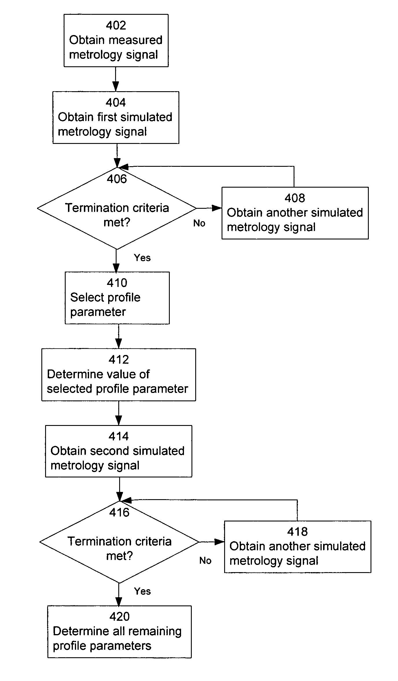
[0024]The following description sets forth numerous specific configurations, parameters, and the like. It should be recognized, however, that such description is not intended as a limitation on the scope of the present invention, but is instead provided as a description of exemplary embodiments.

1. Optical Metrology

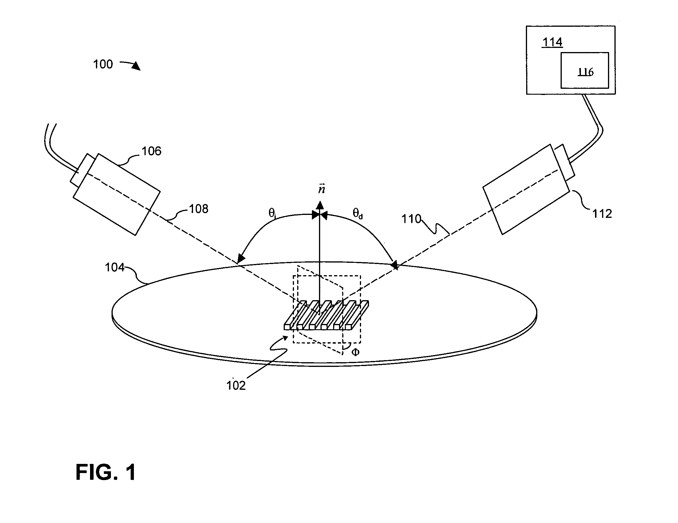
[0025]With reference to FIG. 1, an optical metrology system 100 can be used to examine and analyze a structure formed on a semiconductor wafer. For example, optical metrology system 100 can be used to determine the profile of a grating 102 formed on wafer 104. Grating 102 can be formed in test areas on wafer 104, such as adjacent to a device formed on wafer 104. Alternatively, grating 102 can be formed in an area of the device that does not interfere with the operation of the device or along scribe lines on wafer 104.

[0026]As depicted in FIG. 1, optical metrology system 100 can include a photometric device with a source 106 and a detector 112. Grating 102 is illuminated b...


PUM


Abstract

The profile of an integrated circuit structure is determined by obtaining a measured metrology signal and a first simulated metrology signal, which has an associated profile model of the structure defined by a set of profile parameters. When the two signals match within a first termination criterion, at least one profile parameter is selected from the set of profile parameters. A value for the selected profile parameter is determined. A second simulated metrology signal having an associated profile model of the structure defined by a set of profile parameters with at least one profile parameter equal or close to the determined value for the selected profile parameter is obtained. When the measured and the second simulated metrology signals match within a second termination criterion, values for one or more remaining profile parameters are determined from the set of profile parameters associated with the second simulated metrology signal.

Description

BACKGROUND[0001]1. Field of Invention[0002]The present application relates to integrated circuit (IC) metrology and more particularly to the use of metrology systems and profile modeling to determine the profiles of IC structures.[0003]2. Related Art[0004]With the current drive towards smaller geometries of IC features, feature measurement is increasingly difficult as the size of the features become smaller. However, knowledge of the dimensions of gratings or structures is essential in order to determine if the dimensions of the features are within the acceptable ranges and if, for example, a particular fabrication process causes the sidewalls of the features to be tapered, vertical, T-topped, undercut, or have footings.[0005]Traditionally, a sample was cleaved and examined with a scanning electron microscope (SEM) or similar device. The cross-section SEM method is typically slow, expensive, and destructive, whereas the critical dimension (CD) SEM method only provides one measuremen...

Claims


Application Information

Patent Timeline
Patent Type & Authority Patents(United States)
IPC IPC(8): G01B11/02G01B11/24G01B11/30G01B15/04G01B21/20G01Q80/00H01L21/66
CPCG01B11/24G01B11/303G03F7/70625
Inventor BAO, JUNWEIVUONG, VIMADRIAGA, MANUELPRAGER, DANIEL
Owner TOKYO ELECTRON LTD
Why Eureka
Try Eureka