Method and system for expanding flash storage device capacity

a flash storage device and capacity expansion technology, applied in the memory field, can solve the problems of limiting density further limits the overall sd card capacity, and the flash controller has a limited number of chip enable signals, so as to achieve the effect of greatly expanding the capacity of the flash storage devi

Inactive Publication Date: 2006-10-24
ELECTRONICS & TELECOMM RES INST +1
View PDF9 Cites 75 Cited by
  • Summary
  • Abstract
  • Description
  • Claims
  • Application Information

AI Technical Summary

Benefits of technology

[0016]Through the use of an allocation logic unit with a Flash controller, a single primary chip enable from an input pin is de-multiplexed into a multiple secondary chip enables for multiple Flash memory dies or chips. In so doing, Flash storage device capacity is greatly expanded.

Problems solved by technology

Space constraints and available Flash memory density are the major obstacles in expanding the capacity of the Flash storage devices. FIG. 1 illustrates top, bottom, short side lateral and long side lateral views of a secure digital (SD) card 10.
The available Flash memory density further limits the overall SD card capacity.
In many instances, due to cost and pin count considerations, a Flash controller has a limited number of chip enable signals.
This limitation imposes a restriction on capacity expansion.
Furthermore, as the demand for Flash storage devices has increased, a shortage of certain types of Flash memory occurs during the course of a year.
Flash types of the most popular density are typically out of supply during the peak seasons.

Method used


Image

  • Method and system for expanding flash storage device capacity
  • Method and system for expanding flash storage device capacity
  • Method and system for expanding flash storage device capacity

Examples


Embodiment Construction

[0025]The present invention relates generally to memories and more particularly to a system and method for expanding the capacity of Flash storage devices. The following description is presented to enable one of ordinary skill in the art to make and use the invention and is provided in the context of a patent application and its requirements. Various modifications to the preferred embodiment will be readily apparent to those skilled in the art and the generic principles herein may be applied to other embodiments. Thus, the present invention is not intended to be limited to the embodiment shown but is to be accorded the widest scope consistent with the principles and features described herein.

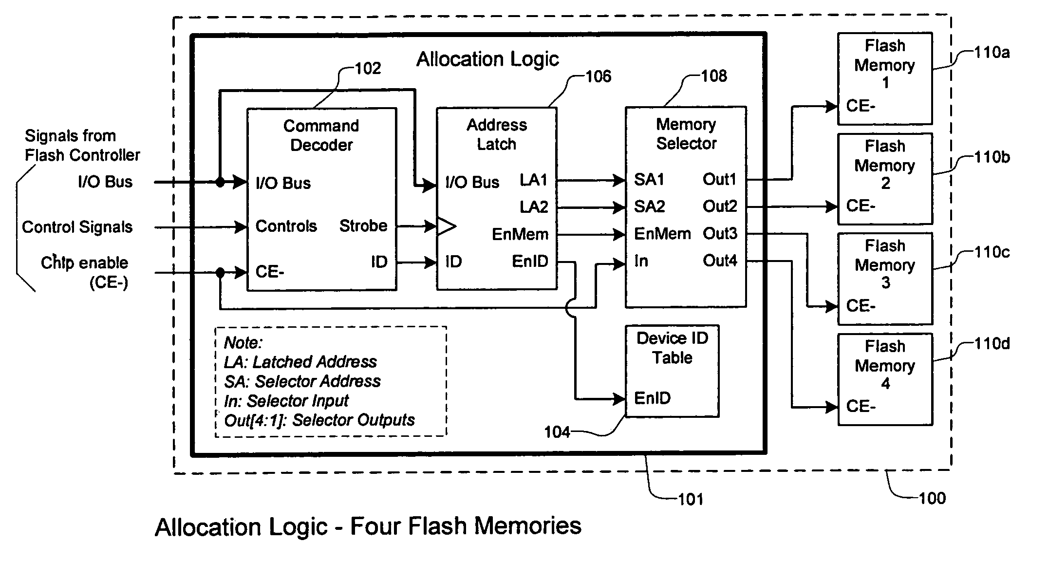
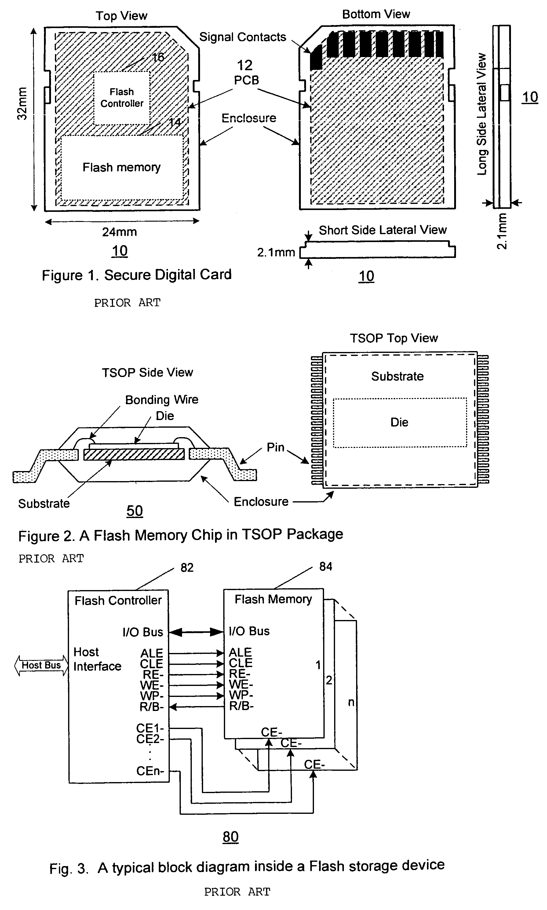
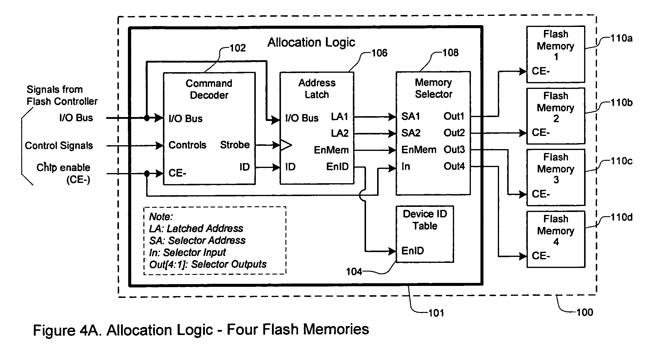
[0026]As before mentioned, a Flash controller has a limited number of chip enables. This limitation imposes a restriction on the capacity expansion of Flash storage devices. A system and method in accordance with the present invention allows for multiple Flash memories to be utilized with a sing...


PUM


Abstract

Through the use of an allocation logic unit with a Flash controller, a single primary chip enable is de-multiplexed into a multiple secondary chip enables for multiple Flash memory dies or chips. In so doing, Flash storage device capacity is greatly expanded. In a first aspect, a memory package includes a plurality of memories; and an allocation logic unit coupled to the plurality of memories for receiving a single chip enable signal. The allocation logic unit de-multiplexes the single chip enable signal to a plurality of chip enable signals. Each of the plurality of chip enable signals access to one of the plurality of memories.In a second aspect, a printed circuit board (PCB) includes a Flash controller for providing at least one primary chip enable signal. The PCB also includes a plurality of Flash memory chips and at least one allocation logic unit coupled to at least a portion of the plurality of Flash memory chips and the Flash controller. The allocation logic unit receives the at least one chip enable signal and de-multiplexes the at least one chip enable signal to a plurality of secondary chip enable signals. Each of the plurality of chip enable signals controls access to one of the Flash memory chips.

Description

FIELD OF THE INVENTION[0001]The present invention relates generally to memories and more particularly to a system and method for expanding the capacity of Flash storage devices.BACKGROUND OF THE INVENTION[0002]The nature of non-volatile, vibration-free, small size and low power consumption has made the Flash memory an excellent component to be utilized in various Flash storage devices. Flash storage devices are widely used as memory storage for computer and consumer system products such as notebook, desktop computer, set top box, digital camera, mobile phone, PDA and GPS etc. The increasing demand for more storage in these products has driven the need to expand the capacity of the Flash storage devices.[0003]There are two types of Flash storage devices. The first type has a pre-defined mechanical dimension. This type includes: (a) Secure Digital (SD) card, (b) Multi Media Card (MMC), (c) Memory Stick (MS) card, (d) Compact Flash (CF) card, (e) Express Flash card, (f) Serial ATA Flas...

Claims


Application Information

Patent Timeline
Patent Type & Authority Patents(United States)
IPC IPC(8): G11C8/00G06F12/02G06F12/06G11C16/04G11C7/10G11C5/00G11C11/34G11C16/02
CPCG11C16/02
Inventor SEE, SUN-TECKCHOU, HORNG-YEELEE, CHARLES C.
Owner ELECTRONICS & TELECOMM RES INST
Why Eureka
Try Eureka