Light emitting diode lamp

a technology of light-emitting diodes and lamps, which is applied in the direction of refractors, display devices, lighting and heating apparatus, etc., can solve the problems of deterioration of conversion of light by cups, so as to prevent the inclination of led chips, prevent short circuits, and promote self-alignment.

Inactive Publication Date: 2006-10-31
ROHM CO LTD
View PDF10 Cites 17 Cited by
  • Summary
  • Abstract
  • Description
  • Claims
  • Application Information

AI Technical Summary

Benefits of technology

[0016]Therefore, as compared with the case where the recess is not provided, it is possible to reliably suppress the height variation of the LED chip in the axial direction of the cup due to the variation of the applied amount of solder paste, and the inclination of the LED chip relative to the axis of the cup. Therefore, it is possible to position the LED chip at a predetermined position along the axis of the conical reflective surface of the cup with high accuracy while suppressing the inclination of the LED chip, whereby the light conversion efficiency of the cup can be considerably enhanced.
[0044]As the die bonding material, use may be made of a thermally meltable material, and the outer side surface of the protrusion may be a rough surface such as a satin-finished surface. With such an arrangement, when an excess of the die bonding material applied to the top surface of the protrusion overflows onto the outer side surface, the die bonding material adheres to the rough peripheral surface provided by satin finishing, for example. When the solder paste H is heated thereafter, the solder melted on outer side surface exhibits pump priming effect to promote the flow of the solder melted on the top surface toward the base portion of the protrusion. Therefore, this arrangement can promote the achievement of the self alignment, the prevention of short circuiting, and the prevention of the inclination of the LED chip placed on the top surface.

Problems solved by technology

Also in such a case, the conversion of light by the cup is deteriorated.
Thus, it is difficult to accurately position the center of the LED chip 104 on the axis 108c of the cup 108 or the nearby position, so that the conversion of light by the cup is deteriorated.

Method used


Image

  • Light emitting diode lamp
  • Light emitting diode lamp
  • Light emitting diode lamp

Examples


first embodiment

[0071]FIGS. 1–5 show the present invention.

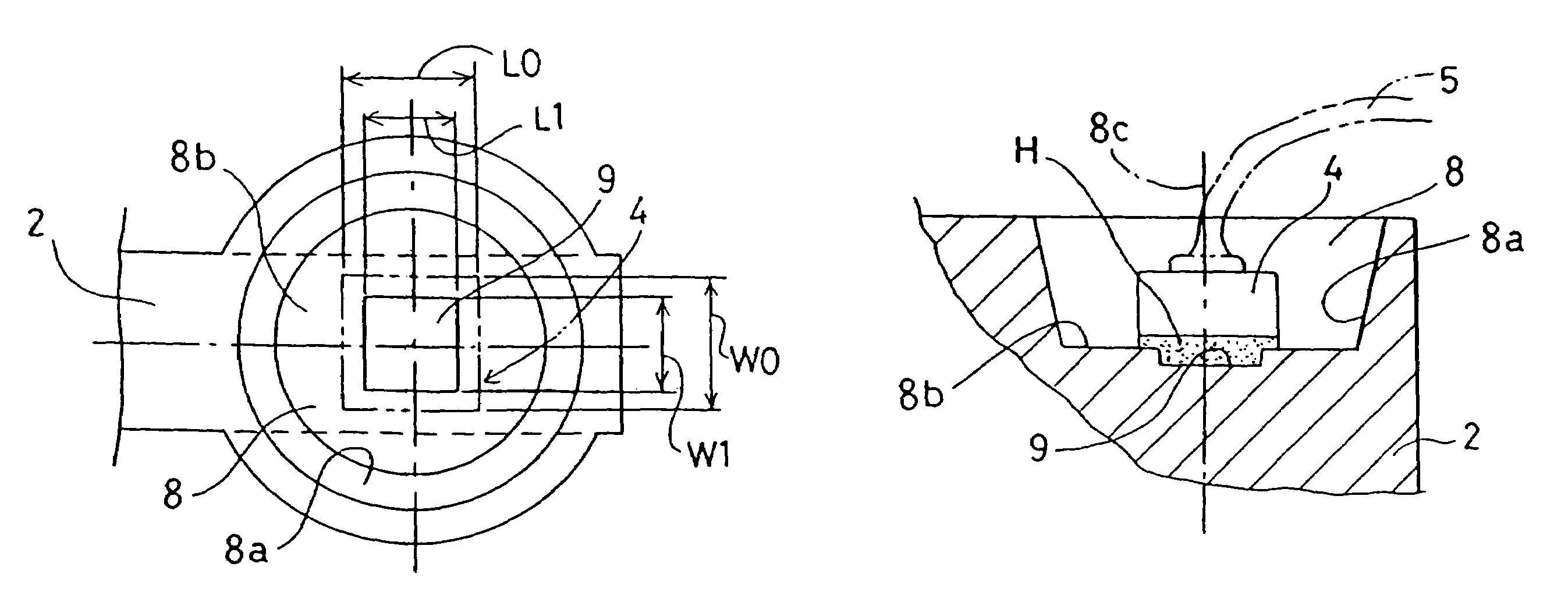
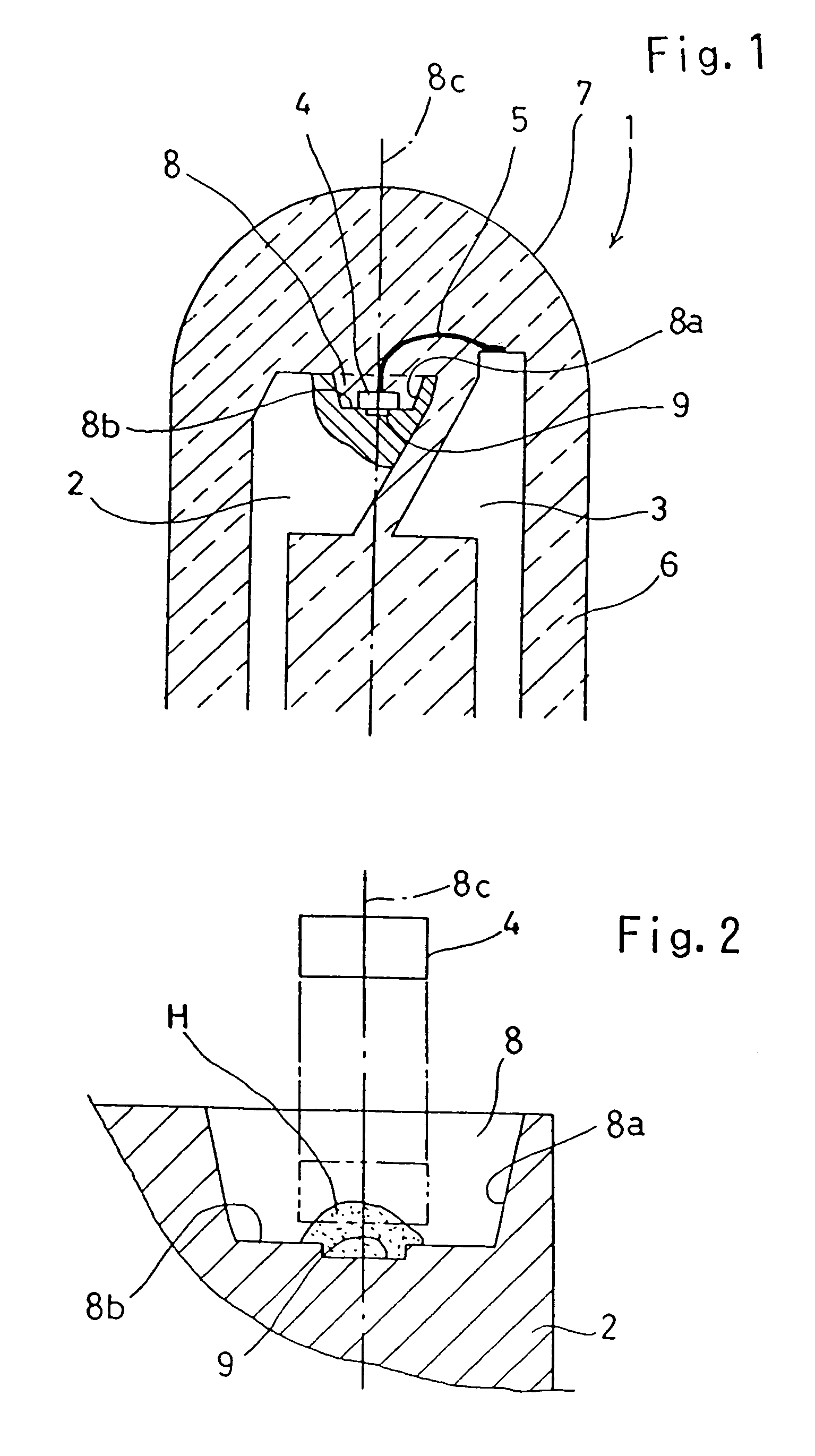
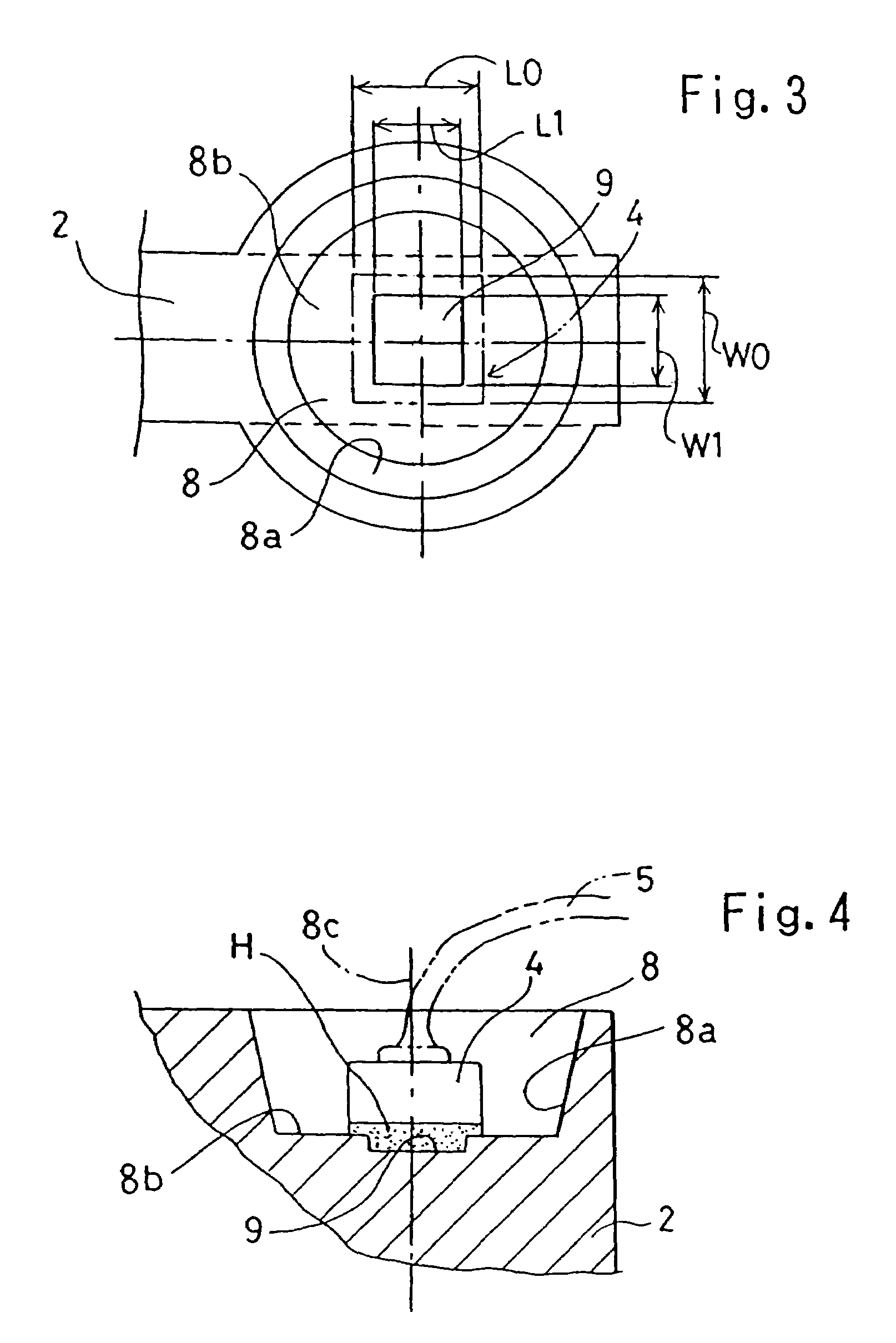
[0072]Indicated by the reference sign 1 in these figures is a light emitting diode lamp. The light emitting diode lamp 1 comprises a pair of lead terminals 2 and 3, an LED chip 4 bonded to a front end of the lead terminal 2, a thin metal wire 5 bonded to the LED chip 4 and the lead terminal 3, and a molded portion 6 made of a transparent synthetic resin for packaging the front ends of the lead terminals 2 and 3. The molded portion 6 has an end integrally formed with a lens portion 7 focusing on the LED chip 4 or the nearby portion.

[0073]To bond the LED chip 4 to the front end of the lead terminal 2, a cup 8 in the form of a recess is formed at the front end of the lead terminal 2. The cup has conical inner circumferential surface formed as a light reflective surface 8a, and a bottom surface 8b formed with a recess 9 of a size which does not receive the LED chip 4.

[0074]Subsequently, an appropriate amount of solder paste H (obtained by mixin...

second embodiment

[0080]FIGS. 6–22 show the present invention.

[0081]Indicated by the reference sign 11 in these figures is a light emitting diode lamp. The light emitting diode lamp 11 comprises a pair of lead terminals 12 and 13, an LED chip 14 bonded to a front end of the lead terminal 12, a thin metal wire 15 bonded to the LED chip 14 and the lead terminal 13, and a molded portion 16 made of a transparent synthetic resin for packaging the front ends of the lead terminals 12 and 13. The molded portion 16 has a front end integrally formed with a lens portion 17 focusing on the LED chip 14 or the nearby portion.

[0082]To bond the LED chip 14 to the front end of the lead terminal 12, a cup 18 in the form of a recess is formed at the front end of the lead terminal 12. The cup has a conical inner circumferential surface formed as a light reflective surface 18a, and a bottom surface 18b integrally formed with a protrusion 19 projecting, like an island, from the bottom surface 18b. An appropriate amount of...


PUM


Abstract

A light emitting diode lamp includes a lead terminal 2 formed with a cup 8 having a conical inner circumferential surface serving as a light reflective surface 8a, an LED chip 4 bonded to a bottom surface 8b of the cup with a die bonding material H, a molded portion 6 made of a transparent synthetic resin for packaging the cup of the lead terminal. The bottom surface 8b of the cup is formed with a recess 9 or a protrusion 19 to which the LED chip 4 is bonded with the die bonding material H, whereby the light conversion efficiency of the conical light reflective surface 8a is enhanced.

Description

BACKGROUND OF THE INVENTION[0001]1. Field of the Invention[0002]The present invention relates to a light emitting diode lamp including a light emitting element packaged with a molded portion made of a transparent synthetic resin.[0003]2. Description of the Related Arts[0004]JP-A 1-152676 and JP-U 62-44530, for example, disclose a light emitting diode lamp of the type described above. Such a light emitting diode lamp generally includes a pair of lead terminals one of which has a front end formed with a cup in the form of an inverted truncated cone. The cup has a conical inner circumferential surface which is made a light reflective surface and a bottom surface on which an LED chip is bonded. The LED chip is connected to the other terminal by wire bonding using a thin metal wire. These elements are packaged by a molded portion made of a transparent synthetic resin and having a lens portion.[0005]Specifically, as shown in FIG. 24 which shows the principal portion as enlarged, such a pr...

Claims


Application Information

Patent Timeline
Patent Type & Authority Patents(United States)
IPC IPC(8): F21V3/00H01L33/60H01L33/62
CPCH01L24/32H01L33/60H01L33/62H01L2224/48091H01L2224/48247H01L2224/48463H01L2224/48465H01L2224/73265H01L2224/92247H01L2924/01013H01L2924/01047H01L2924/01049H01L2924/0105H01L2924/01078H01L2924/01082H01L2924/00014H01L2224/32257H01L2224/32245H01L2924/01005H01L2924/01033H01L2924/00H01L2924/12041Y10S362/80H01L2924/181H01L2224/83385H01L2924/15153H01L2924/00012
Inventor ISOKAWA, SHINJIYAMAGUCHI, TOMOJI
Owner ROHM CO LTD
Why Eureka
Try Eureka