
Method for avoiding transients during switching processes in integrated circuits, and an integrated circuit

Inactive Publication Date: 2006-10-31
INFINEON TECH AG
View PDF13 Cites 0 Cited by
  • Summary
  • Abstract
  • Description
  • Claims
  • Application Information

AI Technical Summary

Benefits of technology

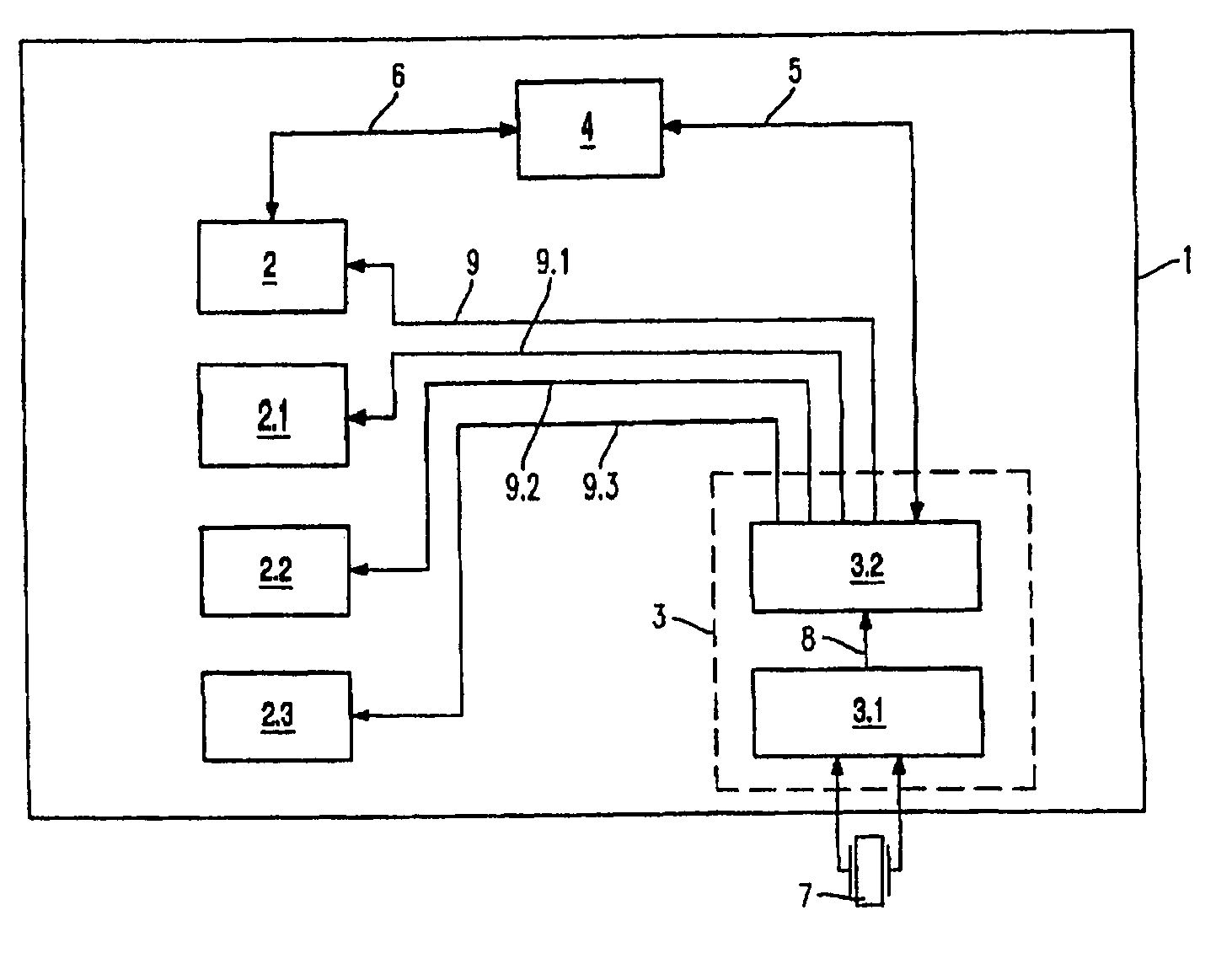
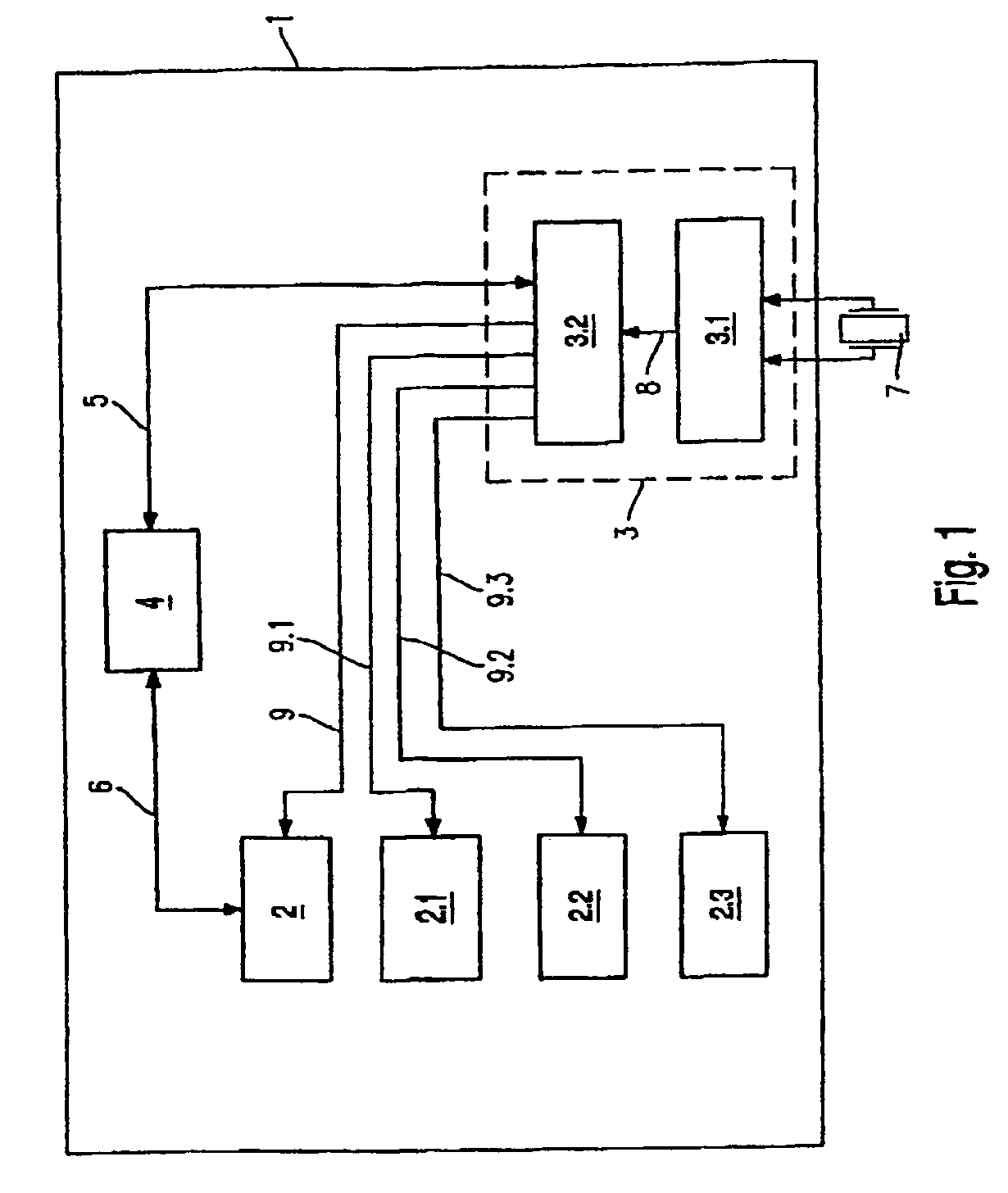
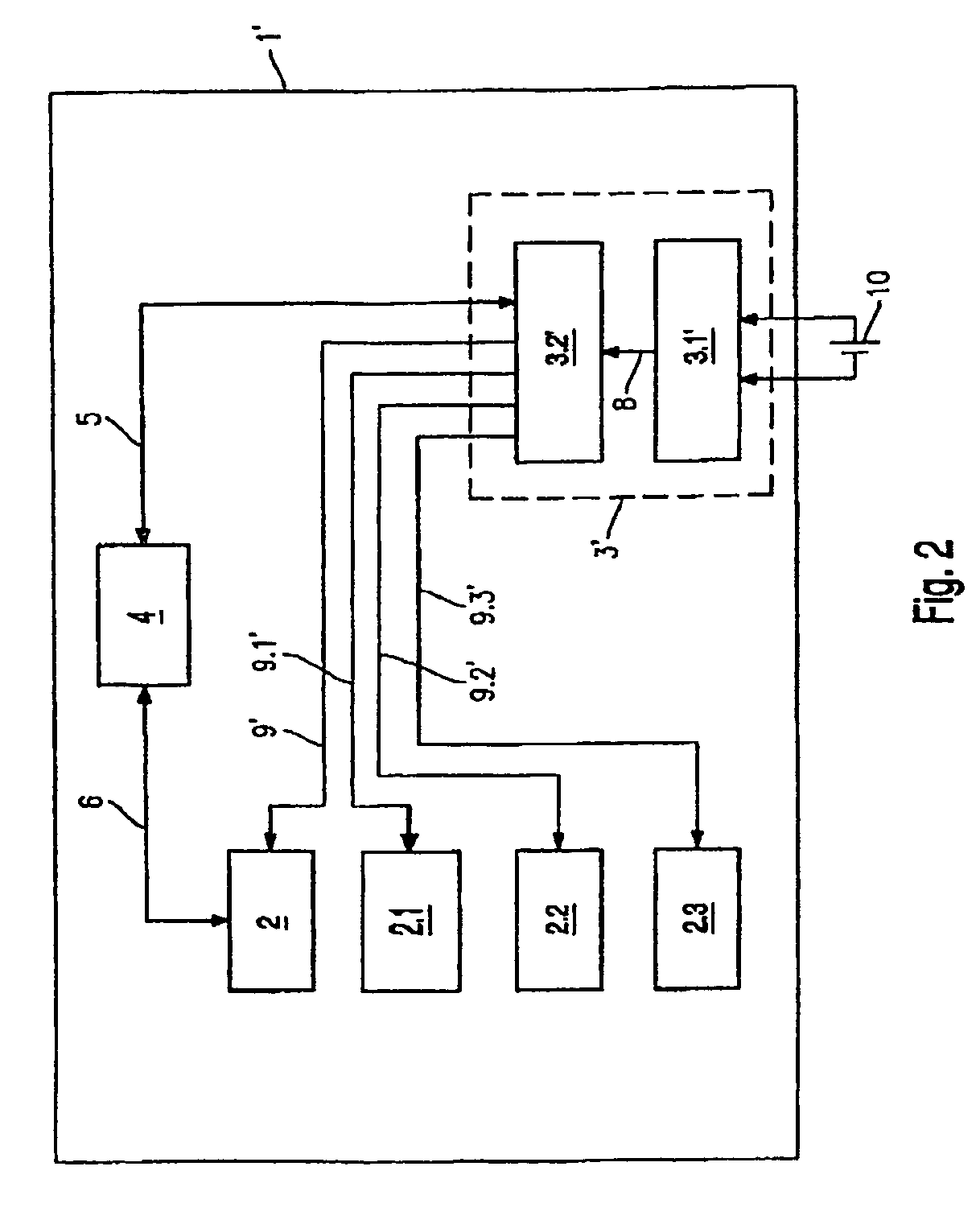
[0006]The invention is based on the object of specifying a method which makes it possible to reduce the harmful influence of transients in integrated circuits. Furthermore, the invention aims to provide an integrated circuit having low susceptibility to disturbances caused by transients.
[0012]In a further second method according to the invention for avoiding transients during switching processes in integrated circuits, the load change occurring during the to the invention, the load change occurring during the switching of the module from the first operating state to the second operating state is essentially compensated for by simultaneous supplementary connection or disconnection of a dummy load. After the supplementary connection of the dummy load, the latter is controlled, with the result that the overall load is reduced. Since the supplementary connection of the dummy load is effected at the same time as the switching of the module, the switching process as such can be abrupt. The occurrence of transients is prevented here by the fact that the overall load change occurring during the switching process remains small. Controlling the magnitude of the dummy load after the connection thereof makes it possible to reduce the overall load, which now again has to be effected “slowly”, i.e. taking account of the lower time limit for changeover processes, since the transient would otherwise occur during the disconnection of the dummy load.

Problems solved by technology

In many cases, e.g. in the case of disconnection of a module, the targeted lengthening of the transition time duration for the switching process is associated with no practical disadvantages.

Method used


Image

  • Method for avoiding transients during switching processes in integrated circuits, and an integrated circuit
  • Method for avoiding transients during switching processes in integrated circuits, and an integrated circuit
  • Method for avoiding transients during switching processes in integrated circuits, and an integrated circuit

Examples


Embodiment Construction

[0025]Modern ICs comprise a multiplicity of components or modules of different complexity and different construction. In this case, in order to obtain higher system integration, analog and digital modules are also realized on one and the same IC. By way of example, an IC may comprise one or more A / D converters, D / A converters, logic units, memory areas and also a microprocessor or a microcontroller as different modules. In the field of mobile radio applications, analog radiofrequency components (e.g. mixing stages) are realized together with digital baseband assemblies (e.g. digital filters) on an IC. A further example of IC-integrated modules is task-specific hardware data paths which execute specific predetermined computation tasks in sequential logic.

[0026]A module in the sense of the invention is thus an essentially autonomous functional unit or assembly in an IC which cooperates with other components or further switchable modules of the IC, the module generally participating in...


PUM


Abstract

In a method for avoiding transients during switching processes in integrated circuits, a module of the integrated circuit is switched from a first operating state to a second operating state, a load change occurring thereby. In this case, it is ensured that the occurring quotient of load change and time duration for the transition from the first operating state to the second operating state does not exceed a predetermined limit value, thereby reducing or avoiding transients associated with such switching.

Description

RELATED APPLICATION[0001]This application is a national stage application of International Application No. PCT / DE02 / 03943 filed Oct. 18, 2002, which is entitled “METHOD FOR AVOIDING TRANSIENTS DURING SWITCHING PROCESSES IN INTEGRATED CIRCUITS, AND AN INTEGRATED CIRCUIT”, which was not published in English, and claims priority to German Patent Application Ser. No. 101 55 428.1, which was filed on Nov. 12, 2001, which is hereby incorporated by reference in its entirety.FIELD OF THE INVENTION[0002]The invention relates to a method for avoiding transients during switching processes in integrated circuits and to an integrated circuit in which measures are taken to avoid transients.BACKGROUND OF THE INVENTION[0003]On account of switching processes, load fluctuations of greater or lesser magnitude occur in integrated circuits (IC). By way of example, load fluctuations are brought about by the occasional activation or deactivation of partial regions or modules of an IC. Such connectable or ...

Claims


Application Information

Patent Timeline
IPC IPC(8): H03K17/16H03K19/003
CPCH03K17/16H03K19/00346
Inventor BOETZEL, ULRICHGERSEMSKY, FRANKHAMMES, MARKUSKRANZ, CHRISTIANLORENZ, RUDIGERNEUBAUER, ANDRESCHMANDT, BERNDWARMERS, MICHAEL
Owner INFINEON TECH AG
Learn More