
System and method for testing circuitry using an externally generated signature

a technology of external generated signatures and circuits, applied in the field of integrated circuit testing, can solve the problems of consuming an consuming undesirably large amount of data storage space, and not expending time and expense in completing a chip assembly. the effect of minimizing the amount of data storag

Active Publication Date: 2006-10-31
ADVANTEST CORP
View PDF30 Cites 41 Cited by
  • Summary
  • Abstract
  • Description
  • Claims
  • Application Information

AI Technical Summary

Benefits of technology

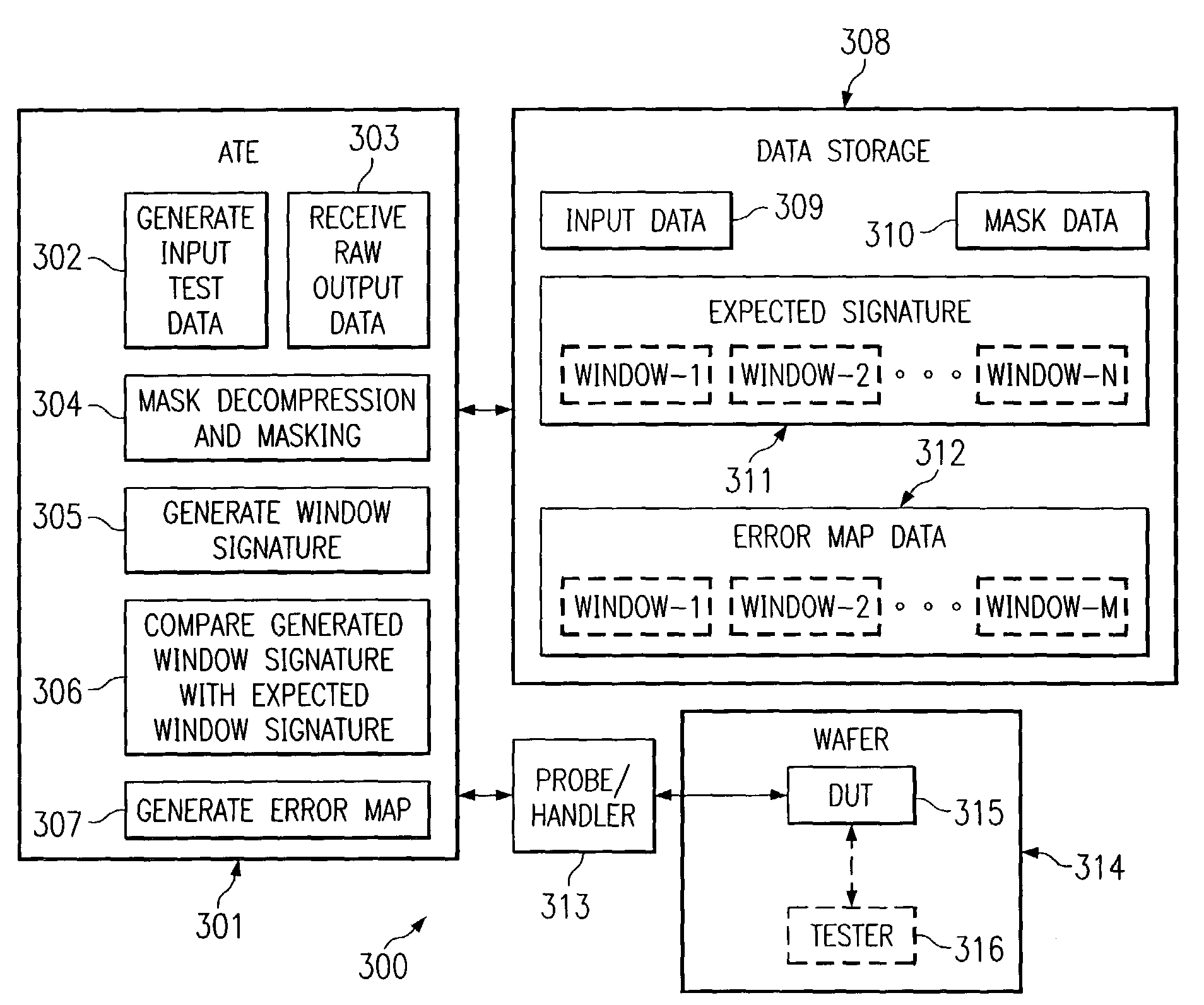
[0021]Further, a preferred embodiment of the present invention may be implemented in combination with mask vector compression and / or input vector compression techniques for a test for further conservation of data storage required for implementing the test. For instance, not only may a signature analysis be implemented for compressing the output vector data, but also input vector and / or mask vector compression techniques may also be implemented in combination therewith for minimizing the amount of data storage required at the ATE for implementing a given test.

Problems solved by technology

That is, if it is determined that a detected defect cannot be repaired, the time and expense of completing a chip assembly will not be expended.
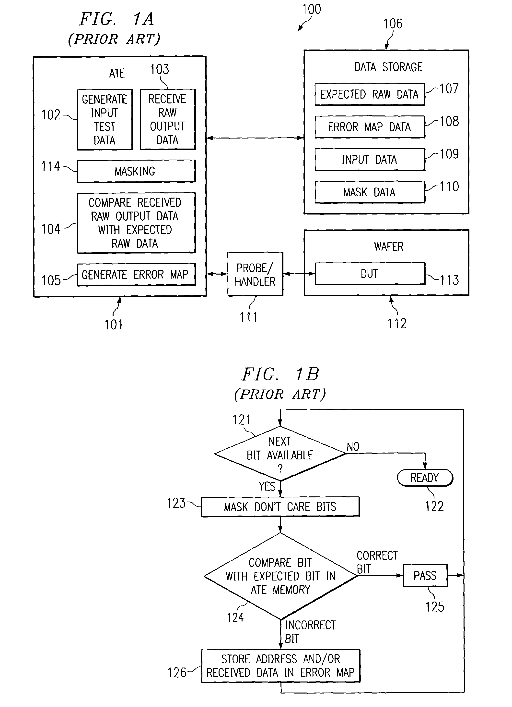
Traditional testing techniques of the existing art require an undesirably large amount of memory on the ATE utilized for the testing, which undesirably increases the cost of the ATE and the resulting product.
Such input vector data, output vector data, and mask vector data for a testing technique may consume an undesirably large amount of data storage space on the ATE.
Further, as the comprehensiveness of a testing technique is increased and / or as the complexity of the device to be tested increases, the amount of data storage space consumed on the ATE for this vector data is likely also increased.
However, truncation of vector sets (e.g., input, output, and mask vector sets), for example, also results in a reduction of test coverage, and as a consequence, may result in reduction of product quality (i.e., truncation reduces the comprehensiveness of the testing of a DUT, which may result in an improperly functioning DUT passing the test).
This reduction in product quality is often not acceptable.
However, in most cases there is still a significant impact on the test coverage.
Thus, diagnosis of errors or error debug is generally limited (e.g., unavailable) when on-chip signature generation is used.
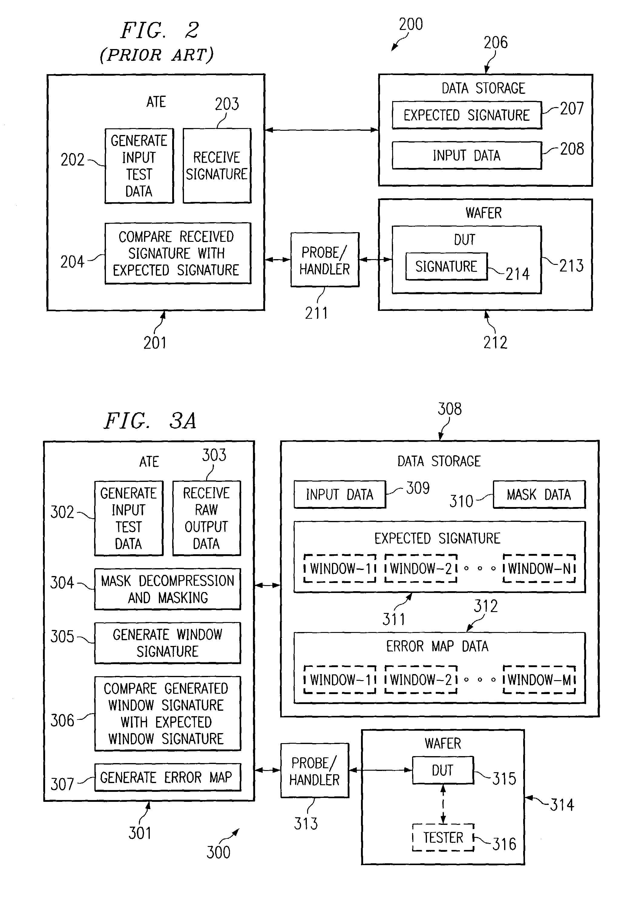
However, on-chip signature analysis techniques of the existing art have several disadvantages.
Such signature generation circuitry consumes area on the chip, thus increasing the overall size of the chip (or decreasing the amount of circuitry that may otherwise be included in the chip) and potentially hindering the chip's performance (e.g., because of the increased distance that signals may be required to travel given the increased size of the chip).
Thus, implementing the signature generation circuitry on-chip is disadvantageous in that it consumes area on the chip (thus increasing the overall size of the chip) and is useful only during-testing of the chip.
Further, as mentioned above, on-chip signature generation is generally disadvantageous because it does not allow for error diagnosis (i.e., a determination as to which one(s) of a group of output bits that have incorrect outputs cannot be made from the signature of such output bits) or error debug.
Further still, on-chip signature generation circuitry may itself have defects.
In certain designs, some flip-flops cannot be scanned due to design constraints.
As a consequence, the values of these non-deterministic bits cannot be controlled without additional design modifications.
However, these design modifications result in area overhead and potential performance degradation.
The presence of unknown / non-deterministic output signals can corrupt the signature, making the signature and the test almost always useless.
The design modifications impact on area, flow, and design performance can be a substantial disadvantage, and not acceptable for some designs.
In addition, in the on-chip signature generation techniques that do not provide on-chip masking capability, the user sometimes desires to perform only a part of the test or suppress certain non-deterministic outputs from the circuitry under test, e.g., during the debugging phase or when certain expected outputs turn out to be simulated incorrectly.
In that case, depending on the number of masked outputs, signature analysis techniques of the existing art cannot be used.
That is, because the signature generation techniques of the existing art comprise on-chip circuitry that is fixed for generating a signature for a certain set of output values, none of such output values can be masked out during the testing process.
Moreover, it is very computationally intensive, and sometimes impossible, to reverse the signature analysis process.
However, it is typically not possible to determine which received bits of the output vector data are wrong.
This seriously limits the error diagnosis / debugging capability of signature-based testing methodologies of the existing art and typically requires a bypass mode for performing error diagnosis / debugging, which adds more circuitry and more inputs / outputs.
For instance, the proposed tester does not allow for concurrent testing and error diagnosis / debugging.
Further, the proposed tester does not allow for masking out of unknown states (e.g., masking of non-deterministic output bits) in generating a signature.
Further, if an ATE were implemented in accordance with such proposal, it would not allow for masking of unknown states, and if such masking were implemented it would require a substantial amount of mask data stored at the ATE (as no compression of the mask data is proposed).
Because of the above-described disadvantages, the use of signature analysis techniques to reduce the ATE memory requirements is not wide spread.

Method used


Image

  • System and method for testing circuitry using an externally generated signature
  • System and method for testing circuitry using an externally generated signature
  • System and method for testing circuitry using an externally generated signature

Examples


Embodiment Construction

[0038]As described above, in typical semiconductor testing, the device under test (DUT) (or “circuitry under test” (CUT)) receives a set of input stimuli from automatic test equipment (ATE) arranged external to the DUT, after which the ATE observes the DUT outputs. In general, the correct expected outputs of the DUT are stored in the ATE memory, and the ATE compares all of the output bits received from the DUT against the stored expected bit values to determine whether the DUT is functioning properly (e.g., whether the DUT is generating the expected output values responsive to the input values).

[0039]In the case of wafer-level testing, a probe may be brought into contact with one or more bonding pads of a die in order to communicate signals (e.g., a test pattern) to the die and to receive the signals output by the die responsive to the input signals. The probe is typically communicatively coupled to an external ATE that is operable to generate the signals to be input to a die and to...


PUM


Abstract

A system and method that enables testing of circuitry using an externally generated signature. An external tester is arranged external to a device under test (DUT). Such external tester is operable to input test data to the DUT, receive output data from the DUT, and generate a signature for at least a portion of such received output data. The external tester compares the generated signature with an expected signature to determine whether the DUT is functioning as expected. If the generated signature fails to match an expected signature, then error data can be written to an error map log. Preferably, further interaction with the DUT is not required after detecting that a generated signature fails to match an expected signature in order to perform such error evaluation. Thus, error evaluation can be performed concurrently with testing of the DUT. Mask data may be stored in a compressed form, and decompressed and used for masking certain non-deterministic output bits in generating the signature.

Description

TECHNICAL FIELD[0001]The present invention relates in general to testing of integrated circuits, and more particularly to a system and method for testing of circuitry utilizing a signature generated external to the circuitry under test.BACKGROUND OF THE INVENTION[0002]During typical semiconductor manufacturing processes, a plurality of integrated circuits are formed as individual dice on a semiconductor wafer. Each semiconductor wafer generally has hundreds to thousands of individual dice formed thereon. Once the dice are formed on a semiconductor wafer, the dice are then tested to determine which dice are functional and which dice are not functional. In most testing procedures, each die is probed using probe equipment while the dice are still on the wafer. This step is also known as “wafer sort.”[0003]The purpose of the wafer-level probe test is to determine, as early as possible in the manufacturing process, whether each individual die is defective or not. The earlier a defective ...

Claims


Application Information

Patent Timeline
IPC IPC(8): G01R31/28G01R31/317G01R31/3183
CPCG01R31/31705G01R31/318307G01R31/318335
Inventor VOLKERINK, ERIK H.KHOCHE, AJAYHILLIGES, KLAUS D.
Owner ADVANTEST CORP
Learn More