

Use of doped silicon dioxide in the fabrication of solar cells
a technology of silicon dioxide and solar cells, applied in the field of solar cells, can solve the problems of associated cost for each step employed in the manufacture of solar cells, and achieve the effect of simplifying the fabrication of solar cells
- Summary
- Abstract
- Description
- Claims
- Application Information
AI Technical Summary
Benefits of technology
Problems solved by technology
Method used
Image

Examples
Embodiment Construction
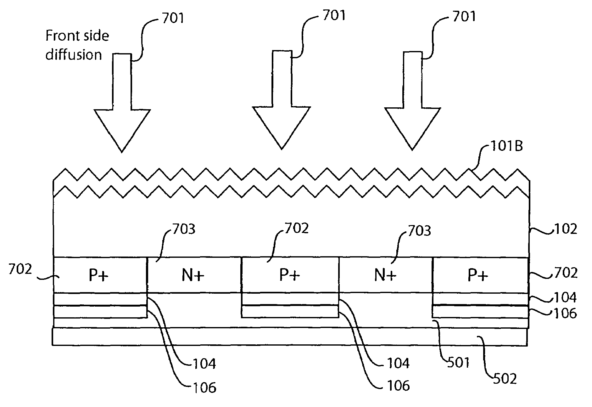
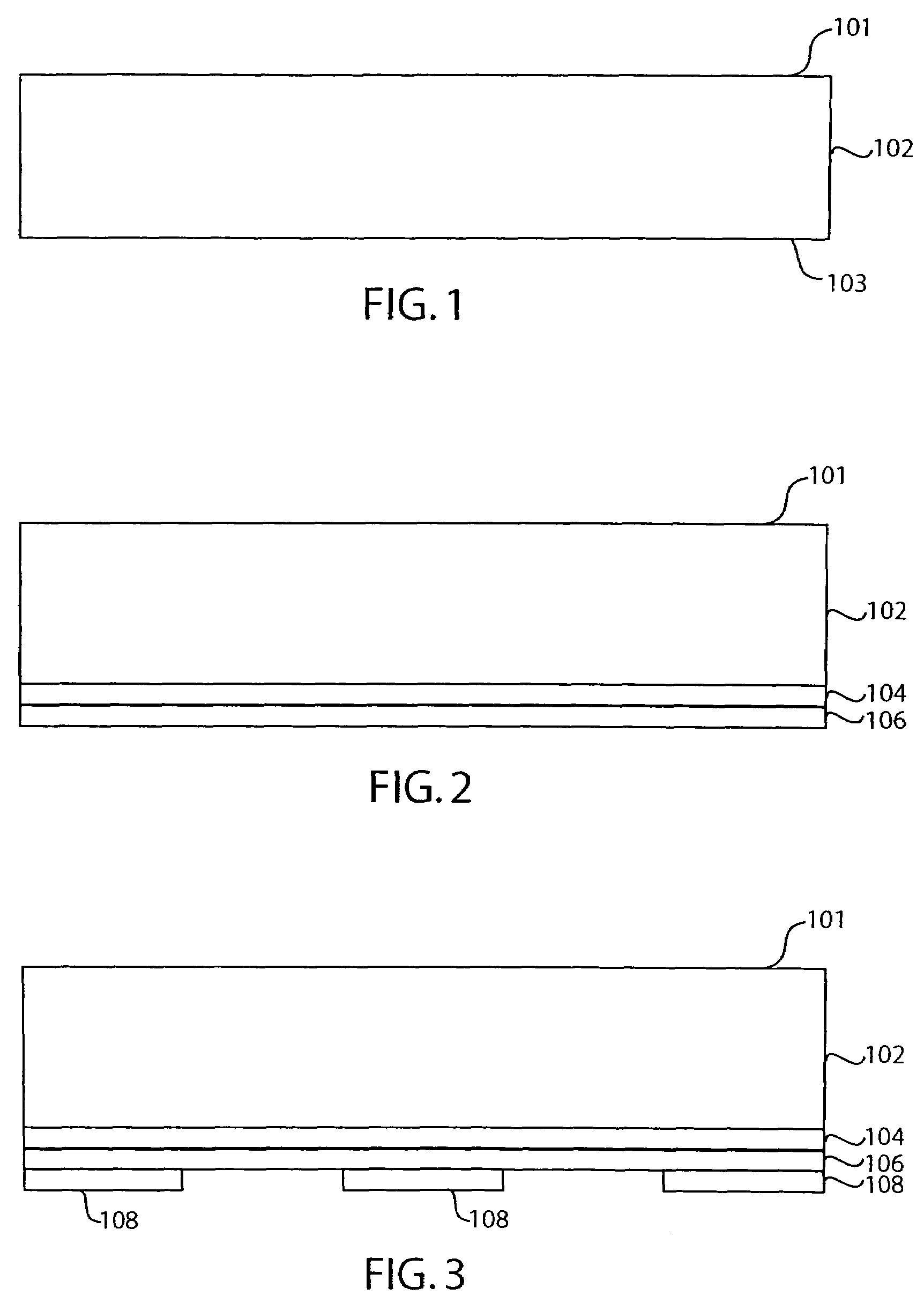
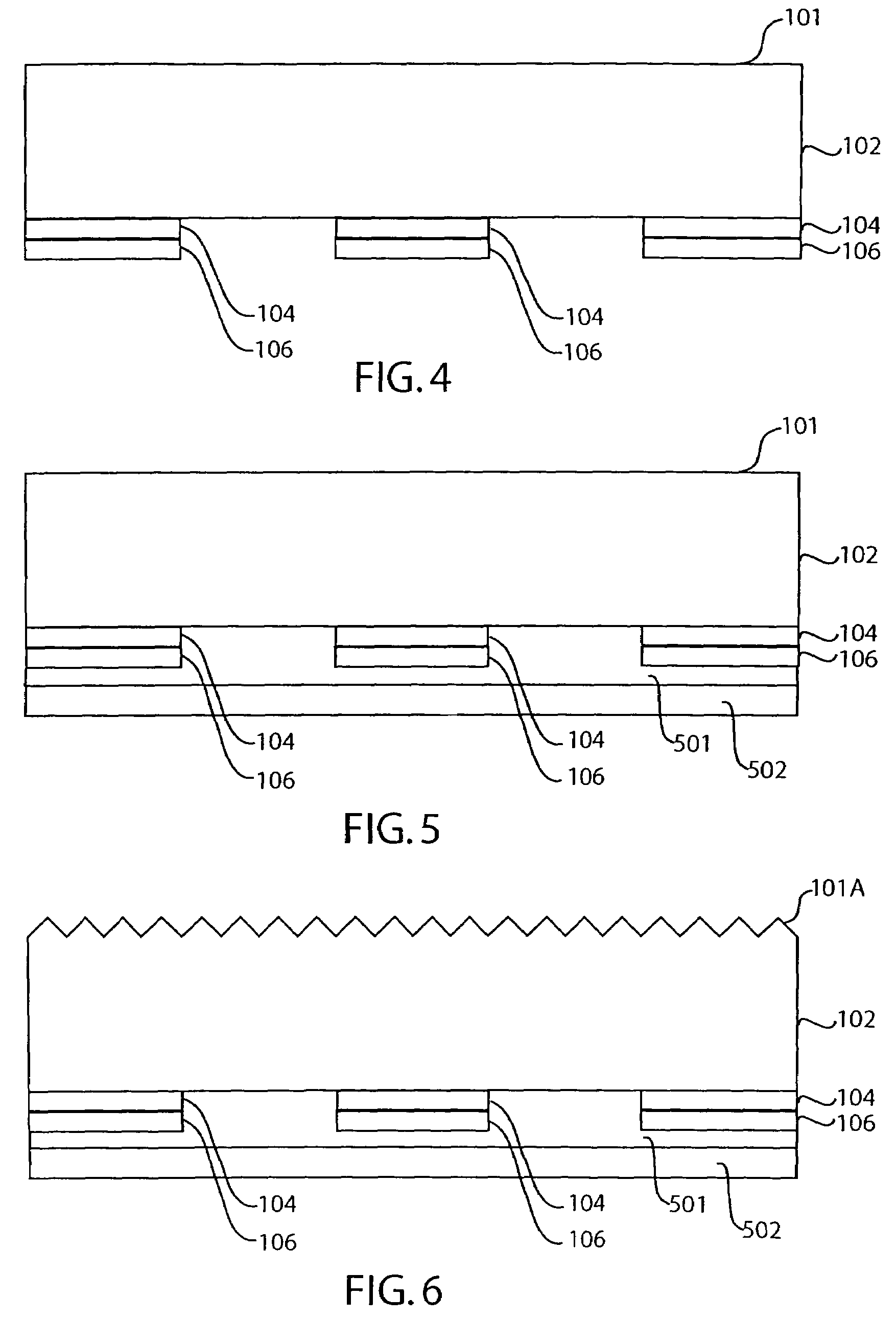
[0011]In the present disclosure, numerous specific details are provided such as examples of apparatus, process parameters, materials, process steps, and structures to provide a thorough understanding of embodiments of the invention. Persons of ordinary skill in the art will recognize, however, that the invention can be practiced without one or more of the specific details. In other instances, well-known details are not shown or described to avoid obscuring aspects of the invention.
[0012]The present disclosure relates to the fabrication of solar cells. Solar cell fabrication processes are also disclosed in the following commonly-assigned disclosures, which are incorporated herein by reference in their entirety: U.S. application Ser. No. 10 / 412,638, entitled “Improved Solar Cell and Method of Manufacture,” filed on Apr. 10, 2003 by William P. Mulligan, Michael J. Cudzinovic, Thomas Pass, David Smith, Neil Kaminar, Keith McIntosh, and Richard M. Swanson; and U.S. application Ser. No. 1...
PUM
 Abstract
Description
Claims
Application Information