Metal barrier integrity via use of a novel two step PVD-ALD deposition procedure

a metal barrier and two-step technology, applied in semiconductor/solid-state device manufacturing, basic electric elements, electric devices, etc., can solve problems such as undesired pinhole formation in the low k imd layer

Inactive Publication Date: 2006-11-14
TAIWAN SEMICON MFG CO LTD
View PDF11 Cites 4 Cited by
  • Summary
  • Abstract
  • Description
  • Claims
  • Application Information

AI Technical Summary

Problems solved by technology

However the use of ALD procedures include precursor sequences using such materials as TiCl4 and NH3 which can p...

Method used


Image

  • Metal barrier integrity via use of a novel two step PVD-ALD deposition procedure
  • Metal barrier integrity via use of a novel two step PVD-ALD deposition procedure
  • Metal barrier integrity via use of a novel two step PVD-ALD deposition procedure

Examples


Embodiment Construction

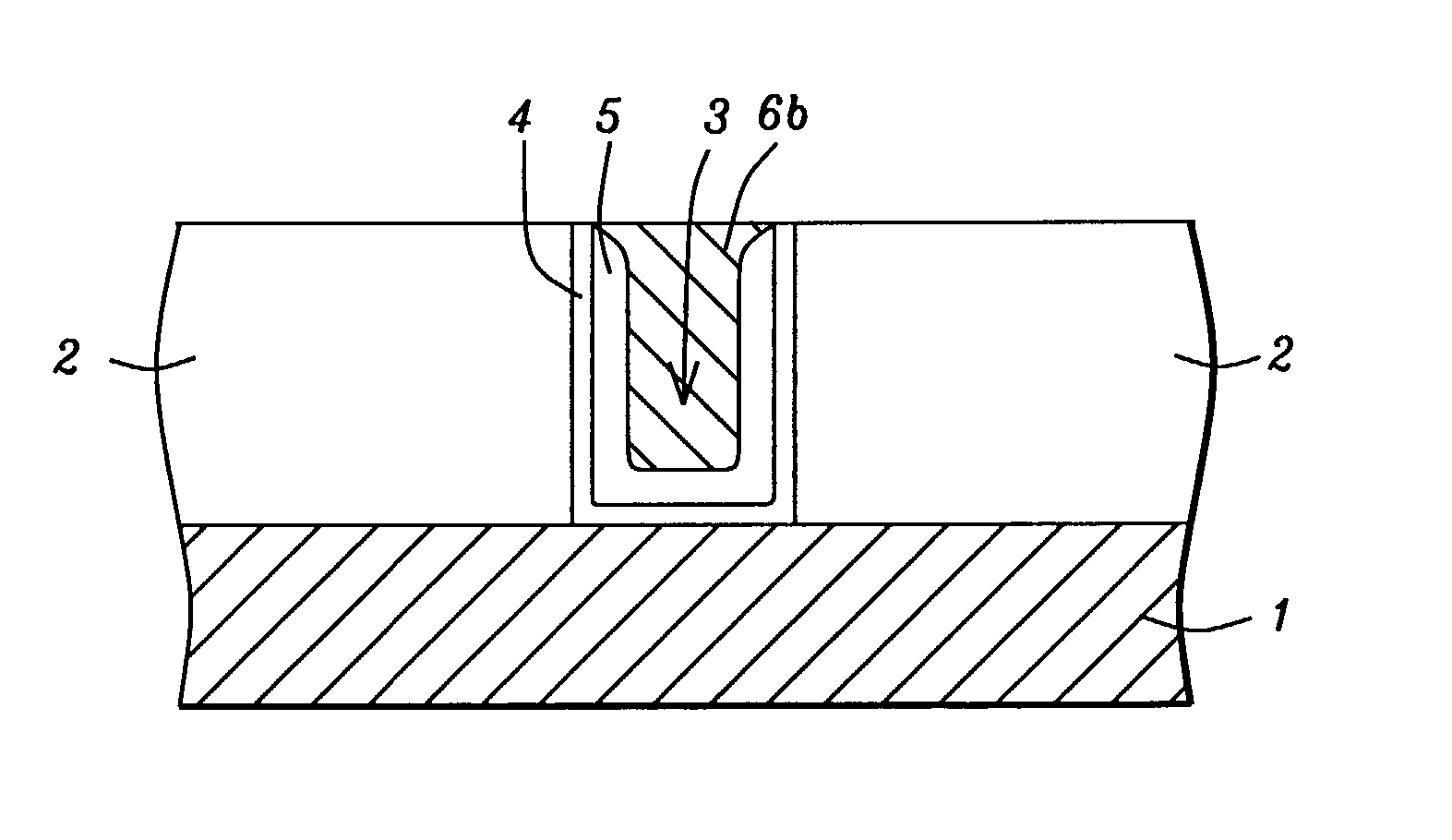
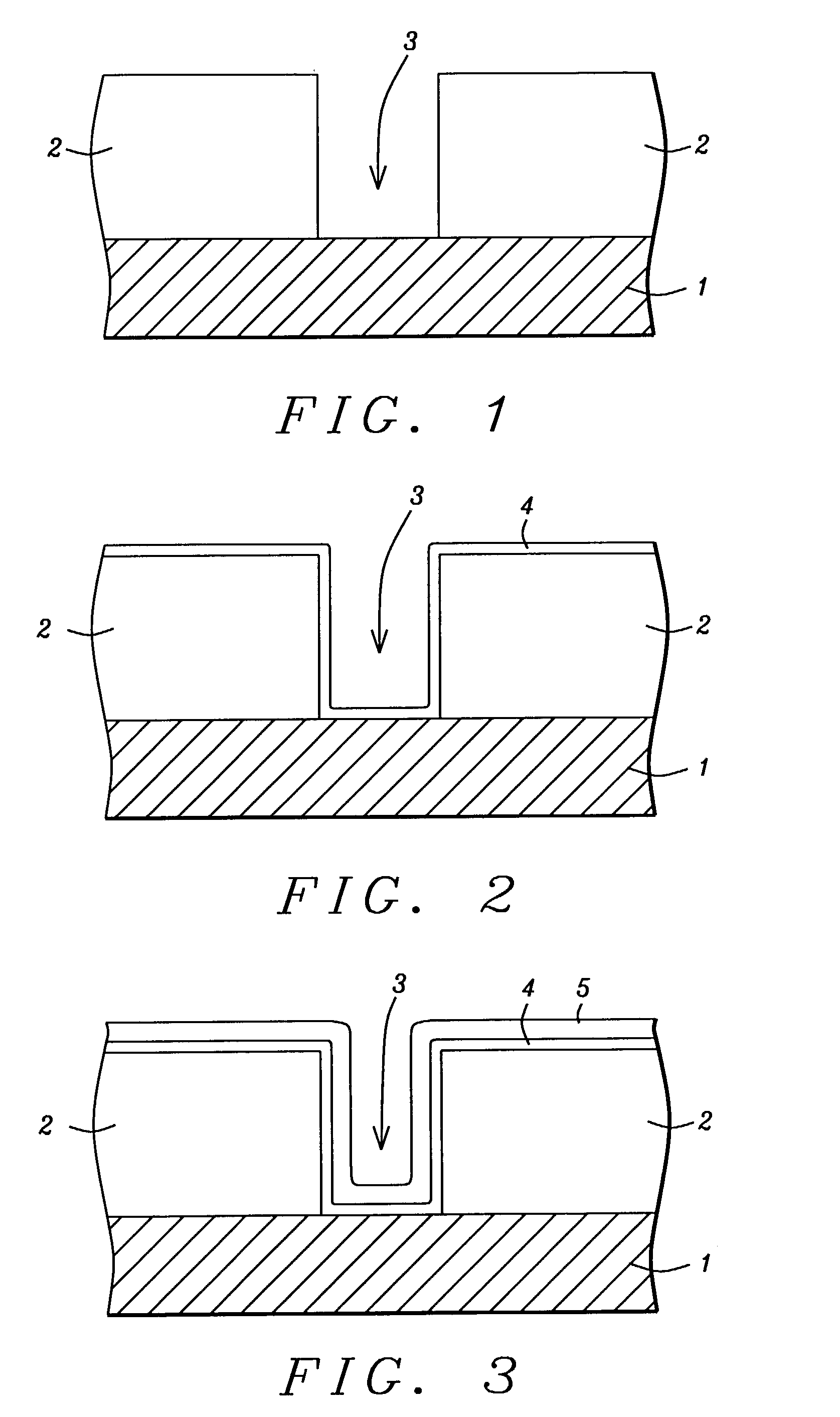
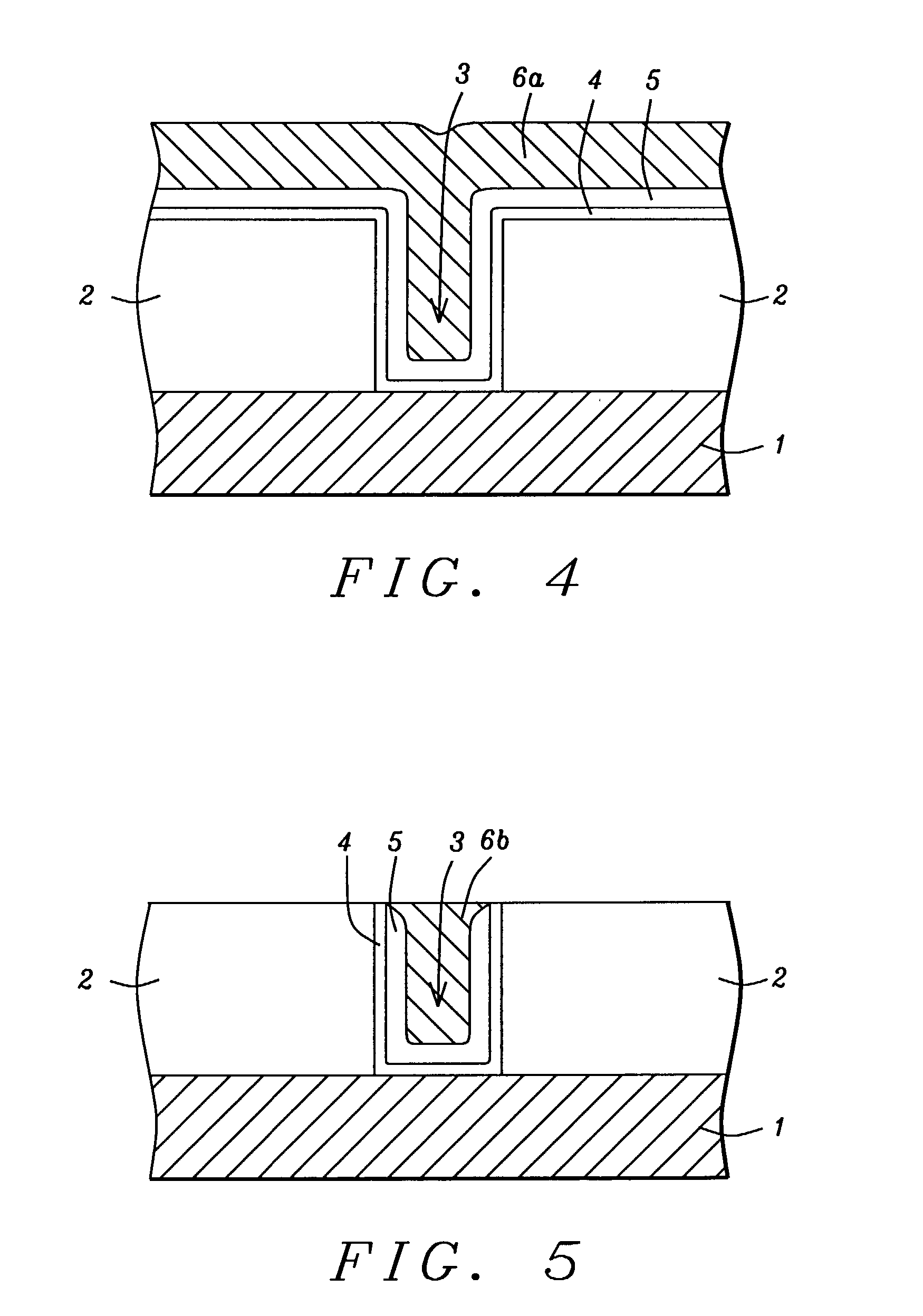
[0012]The method of forming a uniform barrier layer via a two step deposition procedure, on the surfaces of an opening defined in a low k material wherein the opening is used to accommodate a damascene type metal structure, will now be described in detail. Conductive layer 1, shown schematically in FIG. 1, can be a lower level metal interconnect structure or a metal via structure, which in turn communicates with active device regions in a semiconductor substrate. Conductive layer 1, can be comprised of copper, tungsten, or an aluminum based material such as aluminum-copper. Intermetal dielectric (IMD), layer 2, comprised of a low dielectric constant (low k), material such as a fluorinated silicon glass (FSG), or a silicon low k (SiLK) material, is next deposited to a thickness between about 3000 to 7000 Angstroms, via chemical vapor deposition (CVD), procedures. To satisfy performance objectives an IMD layer with a dielectric constant between about 2.5 to 3.0 is chosen. A photoresis...


PUM


Abstract

A method of forming a barrier layer on the surface of an opening defined in a porous, low dielectric constant (low k), layer, has been developed. The method features the use of a two step deposition procedure using a physical vapor deposition (PVD), procedure to initially deposit a thin underlying, first component of the barrier layer, while an atomic layer deposition (ALD), procedure is then employed for deposition of an overlying second barrier layer component. The underlying, thin barrier layer component obtained via PVD procedures is comprised with the desired properties needed to interface the porous, low k layer, while the overlying barrier layer component obtained via ALD procedures exhibits excellent thickness uniformity.

Description

BACKGROUND OF THE INVENTION[0001](1) Field of the Invention[0002]The present invention relates to methods used to fabricate semiconductor devices, and more specifically to a method used to form a barrier layer on the surface of an opening in a low dielectric constant material, wherein the opening is to be used to accommodate a damascene type metal structure.[0003](2) Description of Prior Art[0004]The use of copper interconnect structures, and of low constant dielectric (low k), layers, has allowed increased performance of semiconductor devices to be realized. Resistance decreases resulting from copper interconnect and via structures exhibiting lower sheet resistance than counterpart structures formed from aluminum based materials, in addition to the capacitance reductions obtained via the use of intermetal dielectric (IMD), layers comprised of low k layers such as fluorinated silicon glass (FSG), as well as other silicon low k (SiLK), materials, has allowed the reduction in resistan...

Claims


Application Information

Patent Timeline
IPC IPC(8): H01L21/44H01L21/768
CPCH01L21/76843
Inventor WU, ZHEN-CHENGJANG, SYUN-MING
Owner TAIWAN SEMICON MFG CO LTD
Why Eureka
Try Eureka