
Vertical DRAM and fabrication method thereof

a technology of vertical dram and fabrication method, which is applied in the field of vertical dram, can solve the problems of limiting the improvement of the integration of semiconductor elements, the width of the channel is too narrow, and the performance of the dram is not good, so as to increase the yield of products, increase the width, and increase the integration of the dram

Inactive Publication Date: 2006-11-14
NAN YA TECH
View PDF9 Cites 8 Cited by
  • Summary
  • Abstract
  • Description
  • Claims
  • Application Information

AI Technical Summary

Benefits of technology

The invention provides a vertical DRAM with wider channels of transistors and a related fabrication method to solve the problem of limited space availability. The vertical DRAM comprises a substrate with at least a deep trench, a trench capacitor, a source-isolation oxide layer, and a vertical transistor. The deep trench has an upper trench portion and a lower trench portion separated by the source-isolation oxide layer. The trench capacitor is located in the lower trench portion of the deep trench. The vertical transistor comprises an annular source, an annular drain, a gate conductive layer, and a cylindrical gate dielectric layer. The annular source is located in the substrate next to the source-isolation oxide layer and circularly encompasses the sidewall of the deep trench. The annular drain circularly encompasses the deep trench near the surface of the substrate and is electrically connected to a second contact plug. The annular channel formed when the gate is opened can also have a circular shape as the annular source and drain. The annular channel has an obviously wider width so that the sufficient current of the transistor is raised to match the requirement of DRAM and increase the yield of products. The capacitor and the transistor of a memory cell of the present invention are all filled in the deep trench, and the contact holes for locating contact plugs are fabricated by a self-alignment process, so that the spacing of the occupied area of each of the memory cells can be reduced to further increase the integration of the DRAM.

Problems solved by technology

In a conventional design, the distance between the source and drain occupies larger area and may limit the improvement of the integrations of the semiconductor elements.
However, the prior-art vertical DRAM has a disadvantage that the width of the channel is too narrow, especially when the size of the trench capacitor is smaller 0.1 μm.
A narrow width of the channel may cause the sufficient current to be too small, resulting in a bad performance of the DRAM.

Method used


Image

  • Vertical DRAM and fabrication method thereof
  • Vertical DRAM and fabrication method thereof
  • Vertical DRAM and fabrication method thereof

Examples


Embodiment Construction

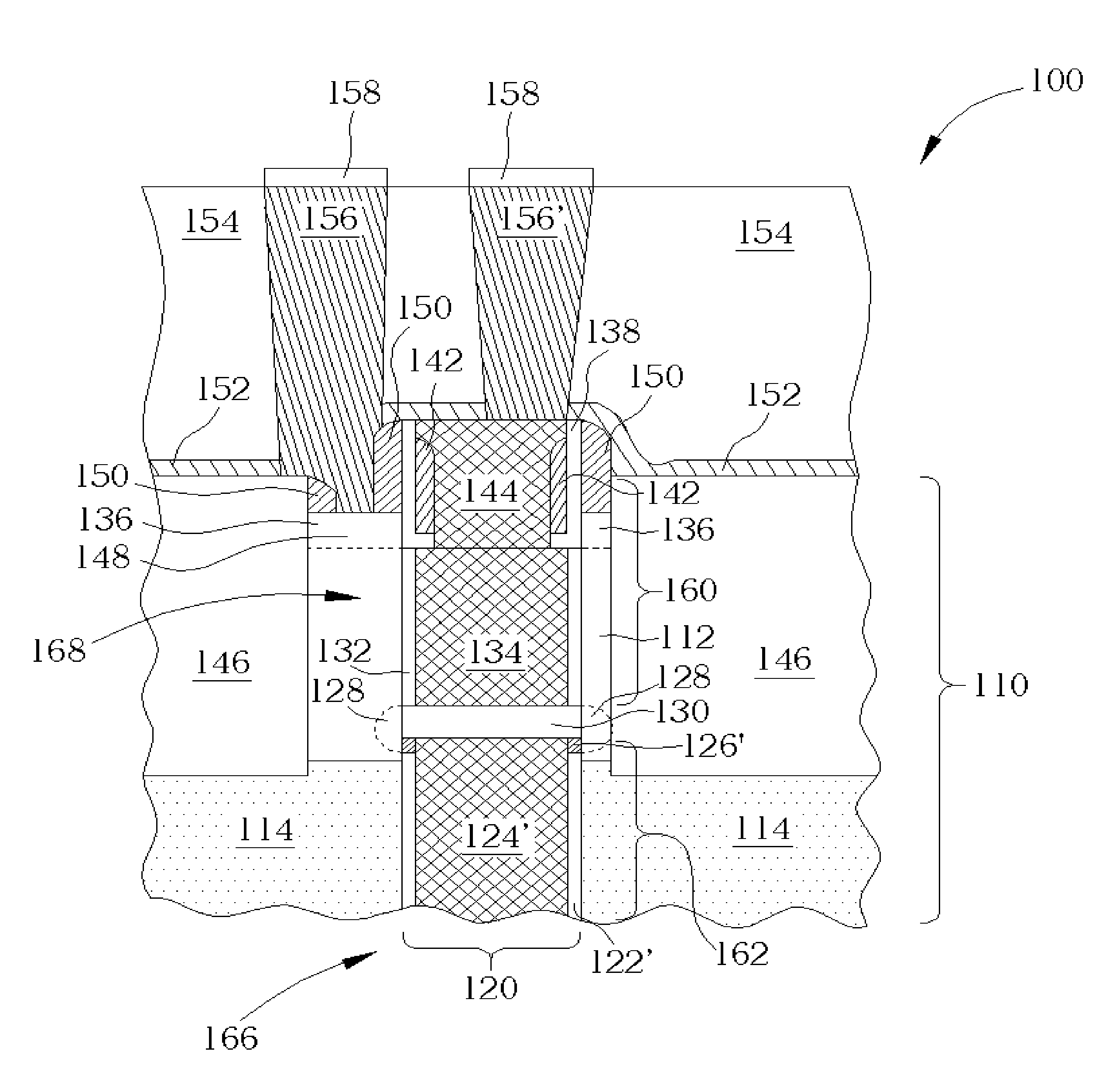
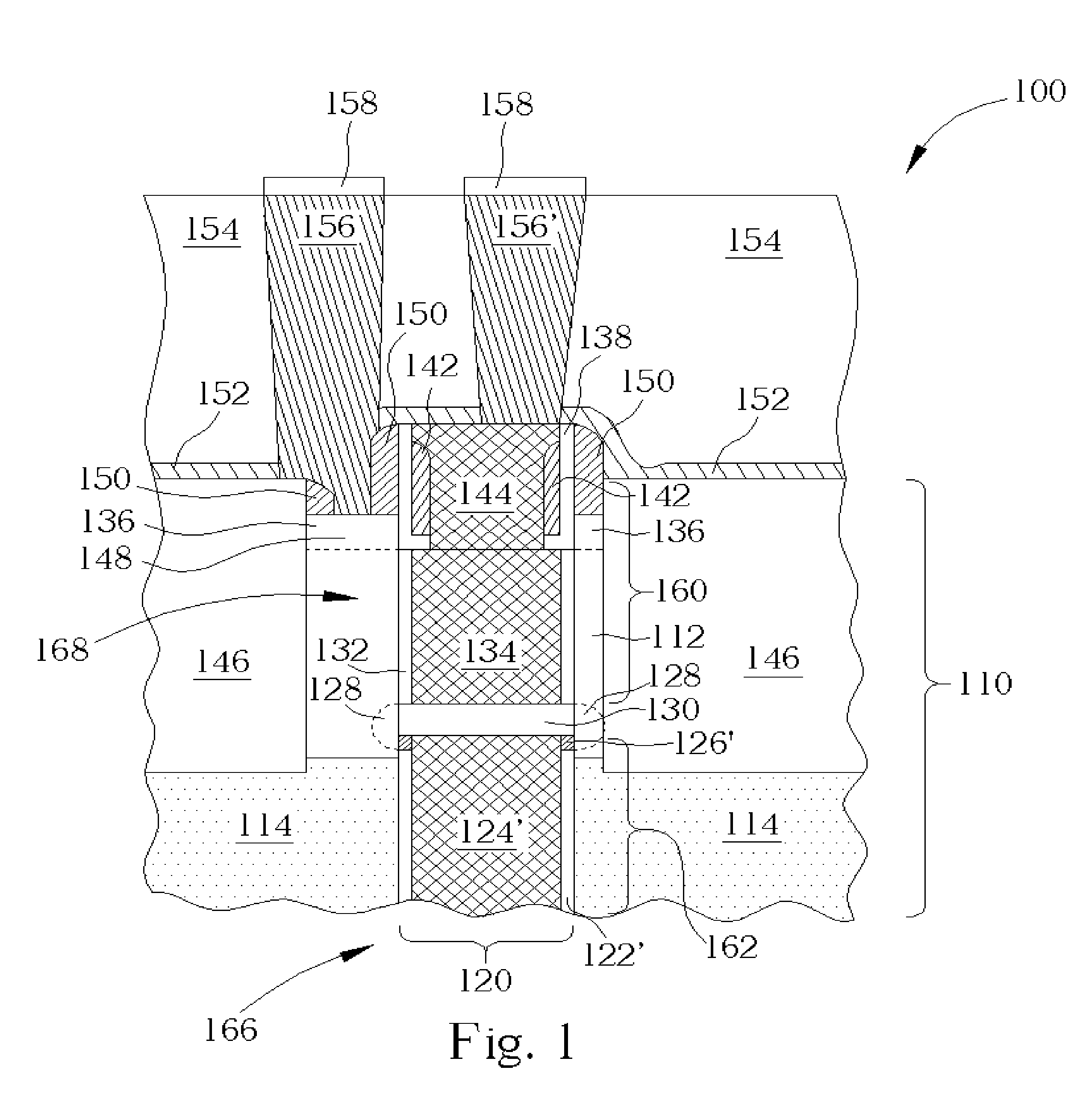
[0013]Please refer to FIG. 1. FIG. 1 is a schematic diagram of a vertical DRAM 100 according to a preferable embodiment of the present invention vertical DRAM. The vertical DRAM 100 comprises a substrate 110 with a plurality of deep trenches 120, a trench capacitor 166 formed in an lower trench portion 162 of the deep trench 120, a vertical transistor 168 formed in an upper trench portion 160 of the deep trench 120, and a source-isolation oxide layer 130 between the vertical transistor 168 and the trench capacitor 166 for isolating the vertical transistor 168 and the trench capacitor 166. The substrate 110 further comprises a P-type well 112. The deep trench 120 locates from the surface of the substrate 110 through the P-type well 112 and extends downward. Each of the memory cells of the vertical DRAM 100 locates in a deep trench 120. The drain and gate of the vertical transistor of each memory are electrically connected to a bit line and a word line (not shown) arranged on the subs...


PUM


Abstract

A vertical DRAM and fabrication method thereof. The vertical DRAM has a plurality of memory cells on a substrate, and each of the memory cells has a trench capacitor, a vertical transistor, and a source-isolation oxide layer in a deep trench. The main advantage of the present invention is to form an annular source diffusion and an annular drain diffusion of the vertical transistor around the sidewall of the deep trench. As a result, when a gate of the transistor is turned on, an annular gate channel is provided. The width of the gate channel of the present invention is therefore increased.

Description

BACKGROUND OF INVENTION[0001]1. Field of the Invention[0002]The invention relates to a vertical DRAM and a fabrication method thereof, and more particularly, to a vertical DRAM with annular sources / drains and annular channels and a fabrication method thereof.[0003]2. Description of the Prior Art[0004]With the development of modern technology, integration circuits and electrical products have been pushed for size reductions to match the trend of high integration and high density. In a conventional planar trench capacitor DRAM, the source, gate, and drain of a MOS transistor are horizontally located on the surface of the substrate. The distance between the source and the drain determines the length and width of the channel of the gate, which is an important factor affecting the design of the size of the MOS transistor. In a conventional design, the distance between the source and drain occupies larger area and may limit the improvement of the integrations of the semiconductor elements...

Claims


Application Information

Patent Timeline
Patent Type & Authority Patents(United States)
IPC IPC(8): H01L27/108H01L29/76H01L29/94H01L31/119H10B12/00
CPCH01L27/10841H01L27/10864H01L27/10876H01L27/10885Y10S257/905Y10S257/908Y10S257/906H10B12/395H10B12/0383H10B12/053H10B12/482
Inventor HSIAO, CHING-NANCHUANG, YING-CHENGLIN, CHI-HUI
Owner NAN YA TECH
Learn More