Liquid crystal display device and manufacturing method therefor

a liquid crystal display and liquid crystal technology, applied in non-linear optics, instruments, optics, etc., can solve the problems of grayscale inversion in half tones, large change in transmittance, narrow viewing angle range, etc., to achieve low black brightness, wide viewing angle range, and high contrast

Inactive Publication Date: 2006-11-14
MITSUBISHI ELECTRIC CORP
View PDF20 Cites 2 Cited by
  • Summary
  • Abstract
  • Description
  • Claims
  • Application Information

AI Technical Summary

Benefits of technology

[0024]In view of the foregoing, it is an object of the present invention to provide a liquid crystal display device with a wide viewing angle range, low black brightness, and high contrast.
[0025]It is another object of the present invention to eliminate light leakage due to the disorder in the orientation of the liquid crystal at step portions or near the base of step portions.
[0027]Consequently, it is possible to eliminate light leakage due to the disorder in the orientation of the liquid crystal at step portions or near the base of step portions.
[0029]Consequently, it is possible to eliminate light leakage due to the disorder in the orientation of the liquid crystal at step portions or near the base of step portions.

Problems solved by technology

In a TN-type liquid crystal display element, there is a large change in transmittance when changing viewing angle based on the operating principles, and the narrow range of the viewing angle is a problem.
Gray-scale inversion in half tones gray is an issue for the viewing angle characteristics.
Consequently, even if an alignment layer is applied in the panel process, the steps cannot be filled in and large steps will be formed in the individual pixels of the liquid crystal display device.
The side walls and bases of the steps become a cause of light leakage because they make it difficult to apply the alignment process by rubbing treatment or the like in the panel process and make it difficult for the liquid crystal to align in the desired direction even when voltage is applied.
For this reason, a normally white type of liquid crystal display device has a structural problem such that, even if sufficient voltage is applied for the black display state, the brightness of the black state becomes high because of the light leakage and this brings about reduced contrast.
On the other hand, there are also problems of gray-scale inversion occurring in half tone grays.

Method used


Image

  • Liquid crystal display device and manufacturing method therefor
  • Liquid crystal display device and manufacturing method therefor
  • Liquid crystal display device and manufacturing method therefor

Examples


first embodiment

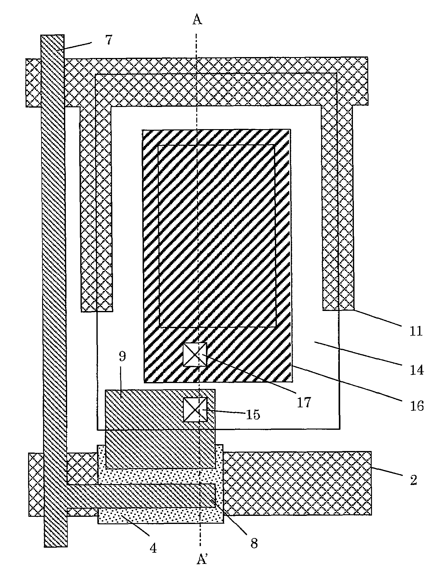
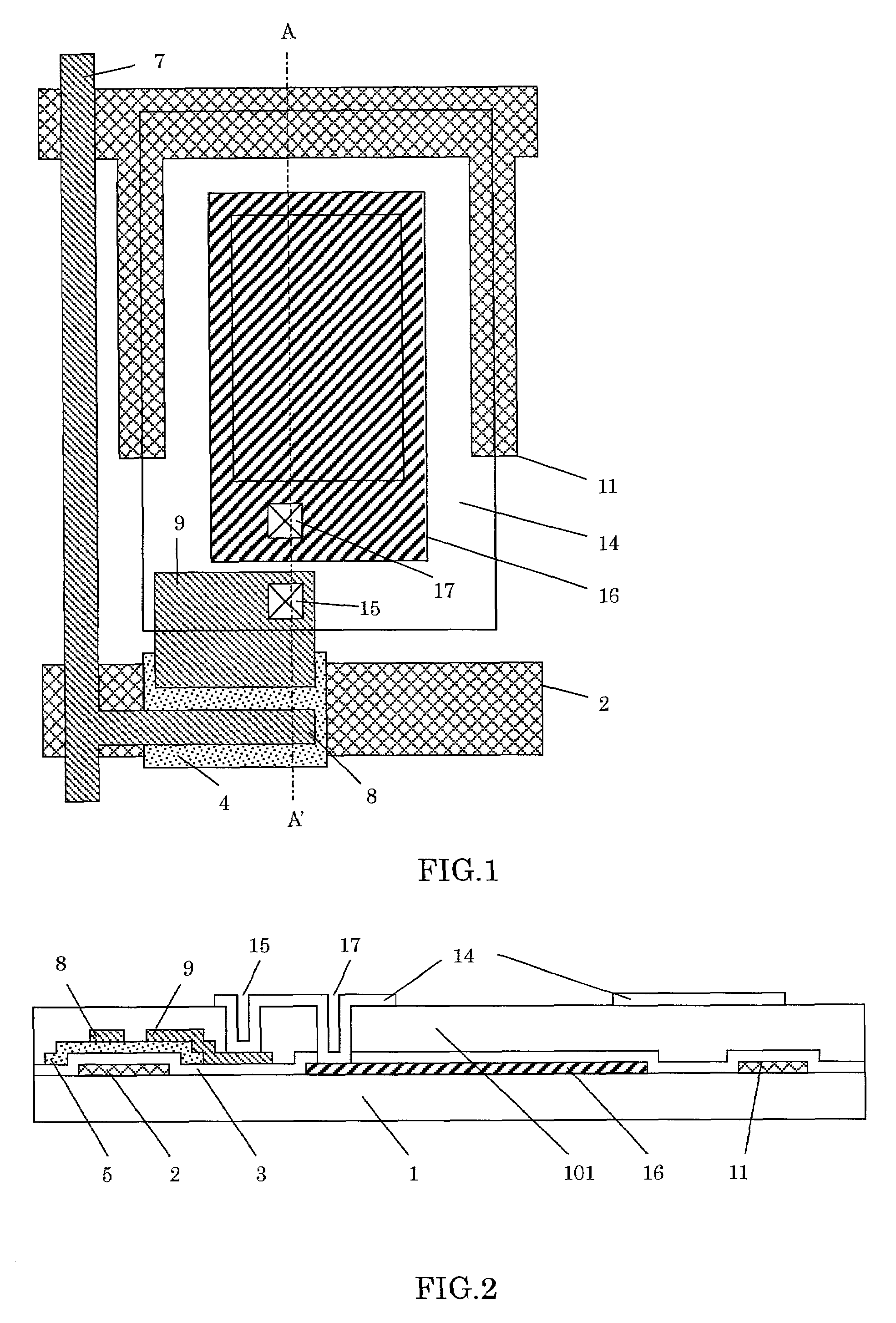
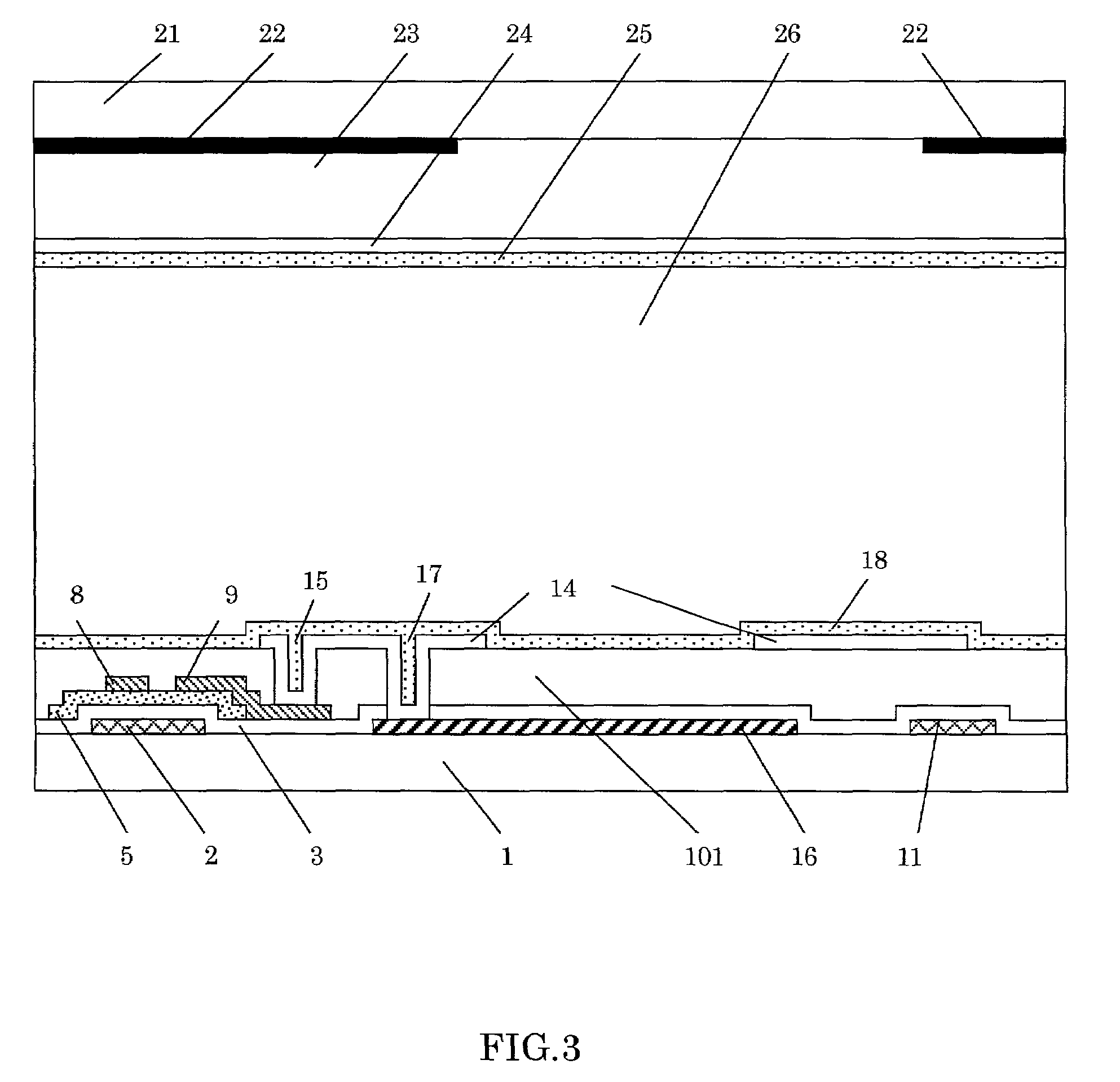
[0058]The active matrix-type liquid crystal display device relating to the first embodiment of the present invention is explained using FIGS. 1, 2, and 3. FIG. 1 shows a plan view of a pixel in a TFT array substrate. FIG. 2 shows a cross sectional view of the pixel in FIG. 1 taken at the line A–A′. FIG. 3 shows a cross sectional, structural view of the display portion of the liquid crystal display device comprising a TFT array substrate, opposite substrate, and liquid crystal.

[0059]In FIG. 1, 2 shows the gate line, 4 shows the semiconductor thin film, 7 shows the source line, 8 shows the source electrode, 9 shows the drain electrode, 11 shows the Cs line, 14 shows the pixel electrode comprising a second layer of ITO, 15 shows the contact of the drain electrode 9 with the pixel electrode 14, 16 shows the pixel electrode comprising a first layer of ITO, and 17 is the contact of the pixel electrode 16 comprising the first layer of ITO with the pixel electrode 14 comprising the second l...

second embodiment

[0066]The active matrix-type liquid crystal display device relating to the second embodiment of the present invention is explained using FIGS. 4 and 5. FIG. 4 is a plan view of a pixel in the TFT array substrate; and FIG. 5 is a cross sectional view of the pixel in FIG. 4 taken at the line A–A′. In FIGS. 4 and 5, elements of the constitution having the same symbols as in FIGS. 1 and 2 show identical portions or portions corresponding to the constitution in FIGS. 1 and 2 and an explanation thereof is omitted. In FIGS. 4 and 5, 2a is the adjacent gate line. In this second embodiment, the cumulative capacitance for stabilizing the pixel potential during the holding period is formed between the pixel electrode 14 and the adjacent preceding gate line 2a.

[0067]The method for manufacturing the liquid crystal display device relating to the second embodiment is explained next. The gate lines 2 and 2a are formed by the sputtering and formation of a metal film on the glass substrate 1, and th...

third embodiment

[0070]The active matrix-type liquid crystal display device relating to the third embodiment of the present invention is explained using FIGS. 6 and 7. FIG. 6 is a plan view of a pixel in the TFT array substrate; and FIG. 7 is a cross sectional view of the pixel in FIG. 6 taken at the line A–A′.

[0071]In FIGS. 6 and 7, elements of the constitution having the same symbols as in FIGS. 1 and 2 show identical portions or portions corresponding to the constitution in FIGS. 1 and 2 and an explanation thereof is omitted. In FIGS. 6 and 7, 2a is the adjacent gate line. In this third embodiment, the storage capacitance for stabilizing the pixel potential during the holding period is formed between the pixel electrode 14 and the Cs line 11, and between the pixel electrode 14 and the adjacent preceding gate line 2a.

[0072]The method for manufacturing the liquid crystal display device relating to the third embodiment is explained next. The gate lines 2 and 2a are formed by the sputtering and form...


PUM

PropertyMeasurementUnit
thicknessaaaaaaaaaa
positive voltageaaaaaaaaaa

Abstract

A liquid crystal display device having transistors disposed at the intersections of gate lines and source lines, pixel electrodes connected with the transistors, opposite electrodes opposite to these pixel electrodes, and liquid crystal held between said opposite electrodes and said pixel electrodes is disclosed. The pixel electrodes comprise a first pixel electrode and a second pixel electrode. The second pixel electrode are disposed in a layer above an insulating layer which is itself disposed in a layer above the first pixel electrode. The second pixel electrode has a region that does not overlap with the first pixel electrode. The second pixel electrode are electrically connected with the first pixel electrode.

Description

BACKGROUND OF THE INVENTION[0001]1. Field of the Invention[0002]The present invention relates to a matrix-type liquid crystal display device, and is more particularly associated with technology relating to the viewing angle characteristics of this liquid crystal display device.[0003]2. Description of the Related Art[0004]A matrix-type display device such as a liquid crystal display device usually comprises two substrates: a thin film transistor array substrate (hereinafter “TFT array substrate”) whereon thin film transistors (hereinafter “TFTs”) and so forth are established, and an opposite substrate whereon a color filter, black matrix, and so forth are established, with a display material such as liquid crystal held between those substrates. Image display is realized by selectively applying voltage to this display material.[0005]FIG. 17 shows an equivalent circuit for a TFT array substrate. As shown in FIG. 17, the pixels are arranged in a matrix. In FIG. 17, G1, G2, and G3 are sc...

Claims


Application Information

Patent Timeline
Patent Type & Authority Patents(United States)
IPC IPC(8): G02F1/1343G02F1/1362G02F1/1368
CPCG02F1/136213G02F1/136227G02F2001/134345G02F2201/123G02F1/134345G02F1/1343
Inventor NAKAYAMA, AKIONAGANO, SHINGOMIZUNUMA, MASAYAKOBAYASHI, KAZUHIROKOYAMA, HITOSHI
Owner MITSUBISHI ELECTRIC CORP
Why Eureka
Try Eureka