Diffraction element and optical device

a technology of optical elements and diffraction gratings, which is applied in the direction of optical radiation measurement, instruments, spectrometry/spectrophotometry/monochromators, etc., can solve the problems of large separation performance of diffraction gratings, limitation in mold production, and difficulty in producing tooth-form diffraction gratings, etc., to achieve excellent flexibility in disposing optical elements, high utilization efficiency of light, and large separation

Active Publication Date: 2006-11-28
ASAHI GLASS CO LTD
View PDF12 Cites 43 Cited by
  • Summary
  • Abstract
  • Description
  • Claims
  • Application Information

AI Technical Summary

Benefits of technology

[0011]The present invention has been made under the above circumstances, and it is an object of the present invention to provide a diffraction element having high utilization efficiency of light, providing large separation depending on wavelength, being excellent in flexibility of disposing optical elements, suitable for mass production and excellent in reliability and temperature property.

Problems solved by technology

However, a saw-tooth-form diffraction grating having a large aspect ratio is difficult to produce, and when it is produced with a resin, there are problems such as limitation in producing a mold, transferring capability to the resin or separation capability of the resin from the mold.
Thus, there has been a problem that a diffraction grating having a large separation performance depending on the wavelength required and having a high utilization efficiency of light, can not be obtained with high productivity at low cost.
Further, when a resin material is employed, there has been a problem of reliability such as deterioration of the element under high temperature or high temperature and high humidity, and thus there has been a problem that the element can be used only under limited environmental conditions.
Accordingly, there has been a problem that it is difficult to produce an element having a short period.
Further, the variation of shape due to the error in production process significantly deteriorates the property, and thus, there has been a problem that a diffraction grating having a high light-utilization efficiency can not be produced at high yield.
Accordingly, there has also been a problem that it is difficult to satisfy high diffraction efficiency and large separation of light depending on wavelength by shortening the period (such as about twice) at the same time.

Method used


Image

  • Diffraction element and optical device
  • Diffraction element and optical device
  • Diffraction element and optical device

Examples


example 1

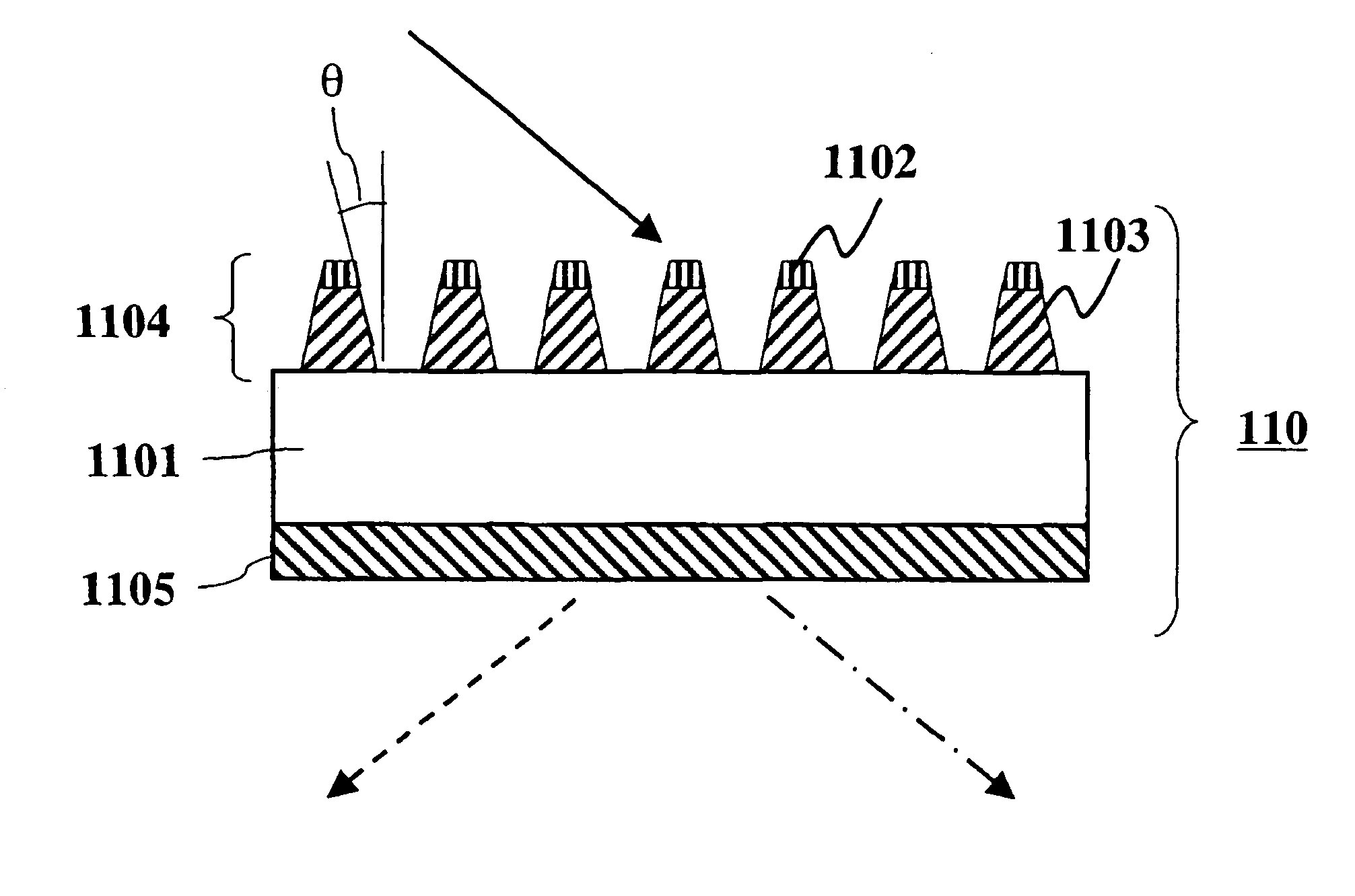
[0075]FIG. 1 is a side view showing the construction of the spectral diffraction element of this example. In this Example, a quartz glass of 2.0 mm thick was used as a transparent substrate 101, and an antireflective film 102 comprising four layers made of TiO2 and SiO2 was provided on a surface of the transparent substrate so that the reflectivity became minimum at an incident angle of 50°. Then, a diffraction grating of rectangular shape was formed by using photolithography and dry etching techniques. Namely, portions of the antireflective film corresponding to recessed portions of the grating were removed by etching first, and then, the quartz glass was etched to have an etching depth of 900 nm, whereby a rectangular diffraction element 103 having a grating period of 1,000 nm in which a multi-layer film was formed on the top of the projecting portions of the quartz glass, was obtained. The proportion of the widths of the recessed portion to the projecting portion was 1:1.

[0076]Th...

example 2

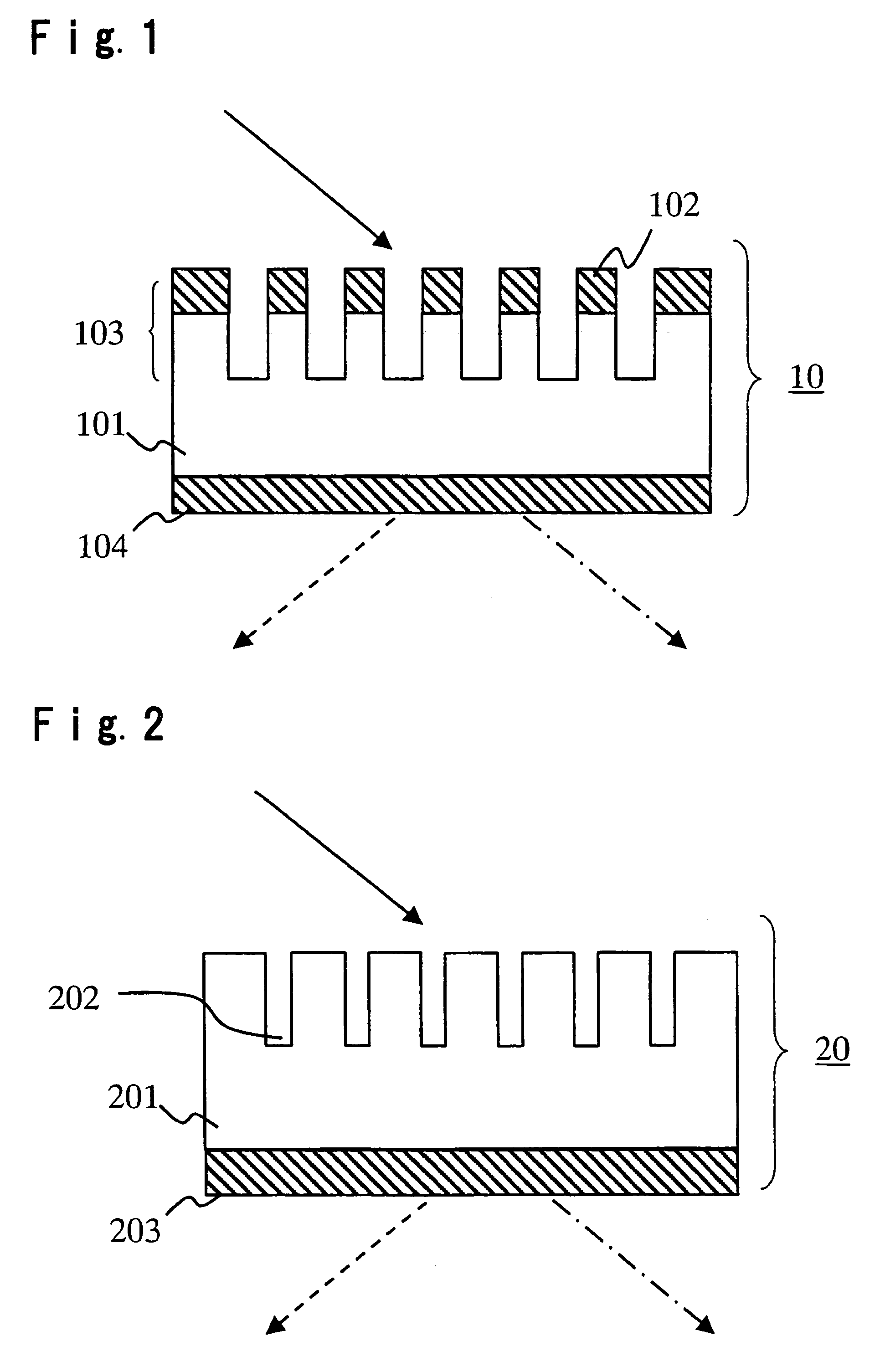
[0078]FIG. 2 is a side view showing the construction of the spectral diffraction element of this example. In this Example, a quartz glass substrate of 2.0 mm thick was used as a transparent substrate 201. The transparent substrate 201 was coated with a photoresist, and a photolithography method was applied using a photomask, not shown, having opening portions with a size of ⅓ of the grating period, to form a photoresist mask in which the proportion of the width of the projecting portion to the recessed portion is 2:1. Then, by using a dry etching technique, a rectangular diffraction grating having a depth of 3,400 nm was formed. Namely, a rectangular diffraction grating 202 having a grating period of 1,500 nm, constituted by projecting portions of 1,000 nm wide and recessed portions of 500 nm wide, and made of a quartz glass having a grating depth of 3,600 nm, was formed.

[0079]Then, on the surface of the transparent substrate 201 opposite from the surface on which the rectangular di...

example 3

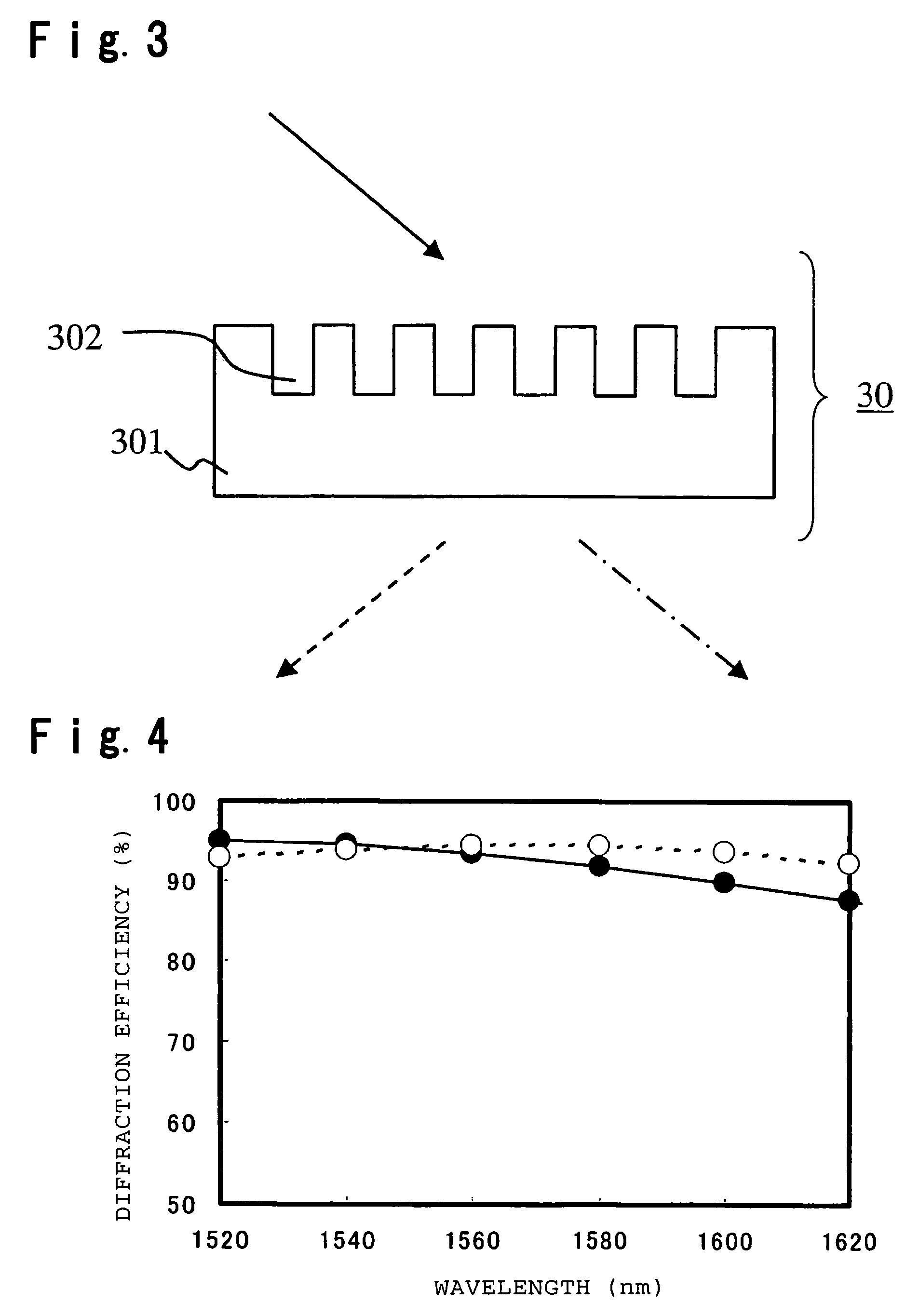
[0081]FIG. 9 is a side view showing the construction of the spectral diffraction element of this example. In this Example, a colorless glass substrate of 2.0 mm thick was used as a transparent substrate 901 and a film of Ta2O5 of 1.3 μm thick and a film of SiO2 of 0.35 μm thick were deposited on a surface of the transparent substrate by a sputtering method. Then, the films thus formed were selectively removed by using techniques of photolithography and dry etching to form a rectangular diffraction grating 904 comprising a Ta2O5 layer 903 and a SiO2 layer 902. In this step, the proportion of the exposed portion to unexposed portion was adjusted by optimizing the opening of a photomask, not shown, to be used for the exposure, so that the proportion between the grating recessed and projecting portions in a grating period became 6:4, namely, the projecting portion became 600 nm and the recessed portion became 400 nm.

[0082]Then, on the other surface of the transparent substrate 901 oppos...


PUM


Abstract

A diffraction element having high diffraction efficiency and large wavelength-separation effect, which is excellent in mass-productivity and is formed by a simple process, is obtained. In a diffraction element having a rectangular grating formed in a surface of a transparent substrate whose cross-section is of an alternating recessed and projecting shape and each of the projecting portions is symmetrical, the period of the grating is equal to or smaller than the wavelength of incident light and the diffraction element is adopted so that the light is incident obliquely to its surface where the grating is formed.

Description

TECHNICAL FIELD[0001]The present invention relates to a diffraction element and an optical device, in particular, to a spectrometry device, and in more detail, to a diffraction element for changing the output direction of light depending on the wavelength, which is to be used for optical multiplex communication or spectrophotometry, and to a spectrometry device employing the diffraction element.BACKGROUND ART[0002]There is a method of diffracting light having various wavelengths into different directions to separate the light depending on the respective wavelengths, and measuring the intensity of each of the separated light to determine the intensity of light of various wavelengths contained in the incident light. Here, in order to utilize the separated light with good efficiency, it is preferred that a diffracted light is efficiently concentrated on a specific diffraction order, and as the method for the wavelength separation, a method of employing a diffraction element having a sa...

Claims


Application Information

Patent Timeline
Patent Type & Authority Patents(United States)
IPC IPC(8): G02B5/18G01J3/18G02B6/34
CPCG01J3/18G02B5/1809G02B5/1857G02B5/1871G02B5/18
Inventor SATO, HIROMASANASHI, HIROTAKA
Owner ASAHI GLASS CO LTD
Why Eureka
Try Eureka