Circuit suitable for vertical integration and method of producing same

a vertical integration and circuit technology, applied in the direction of solid-state device manufacturing, electric devices, semiconductor/solid-state device manufacturing, etc., can solve the problems of changing the properties of the finished active components of the lower level, longer turnaround time for production, and production of front side and backside contacts partly using materials, so as to improve yield and simplify the sequence of production. , the effect of optimizing the running time of the plan

Inactive Publication Date: 2006-12-05
GIESECKE & DEVRIENT GMBH
View PDF14 Cites 4 Cited by
  • Summary
  • Abstract
  • Description
  • Claims
  • Application Information

AI Technical Summary

Benefits of technology

[0008]It is assumed that the vertical electric contacts are produced using process steps in the production of the vertically integratable circuit itself. This simplifies the sequence of production for vertically integratable circuits and thus the three-dimensional integrated circuit as a whole, thereby optimizing plant running times since process steps are sa...

Problems solved by technology

The disadvantage of this method is that the high temperatures during recrystallization can change the properties of the finished active components of the lower level.
Furthermore, the serial processing of the vertically integrated overall circuit results in an accordingly longer turnaround time for production.
The disadvantage of this m...

Method used


Image

  • Circuit suitable for vertical integration and method of producing same
  • Circuit suitable for vertical integration and method of producing same
  • Circuit suitable for vertical integration and method of producing same

Examples


Embodiment Construction

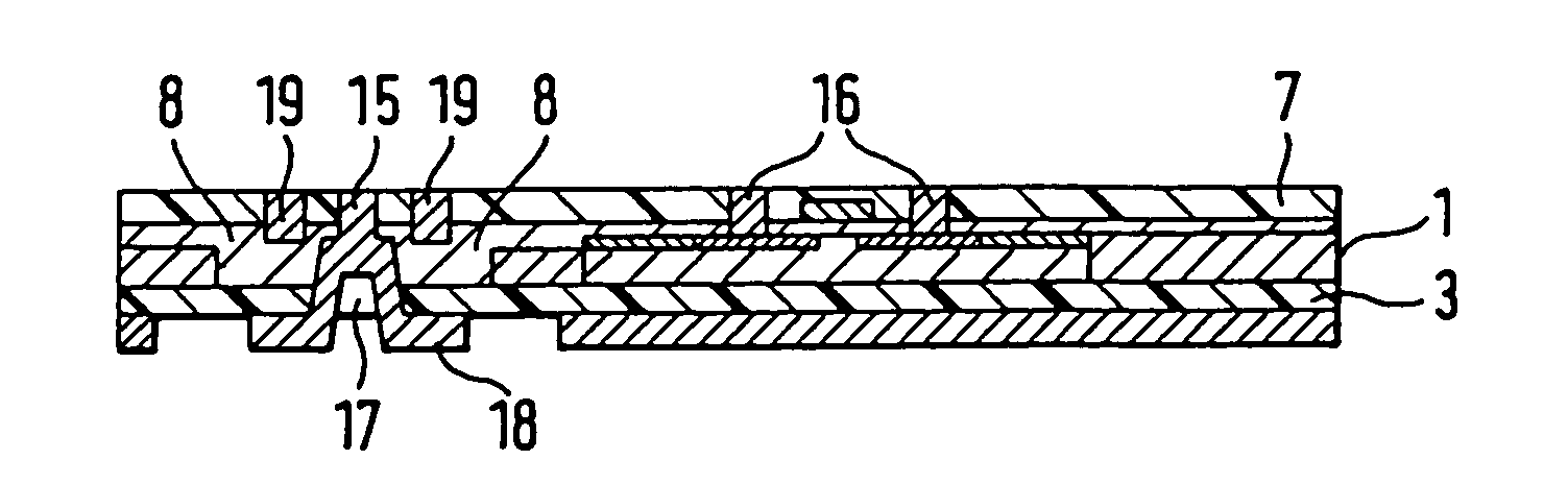
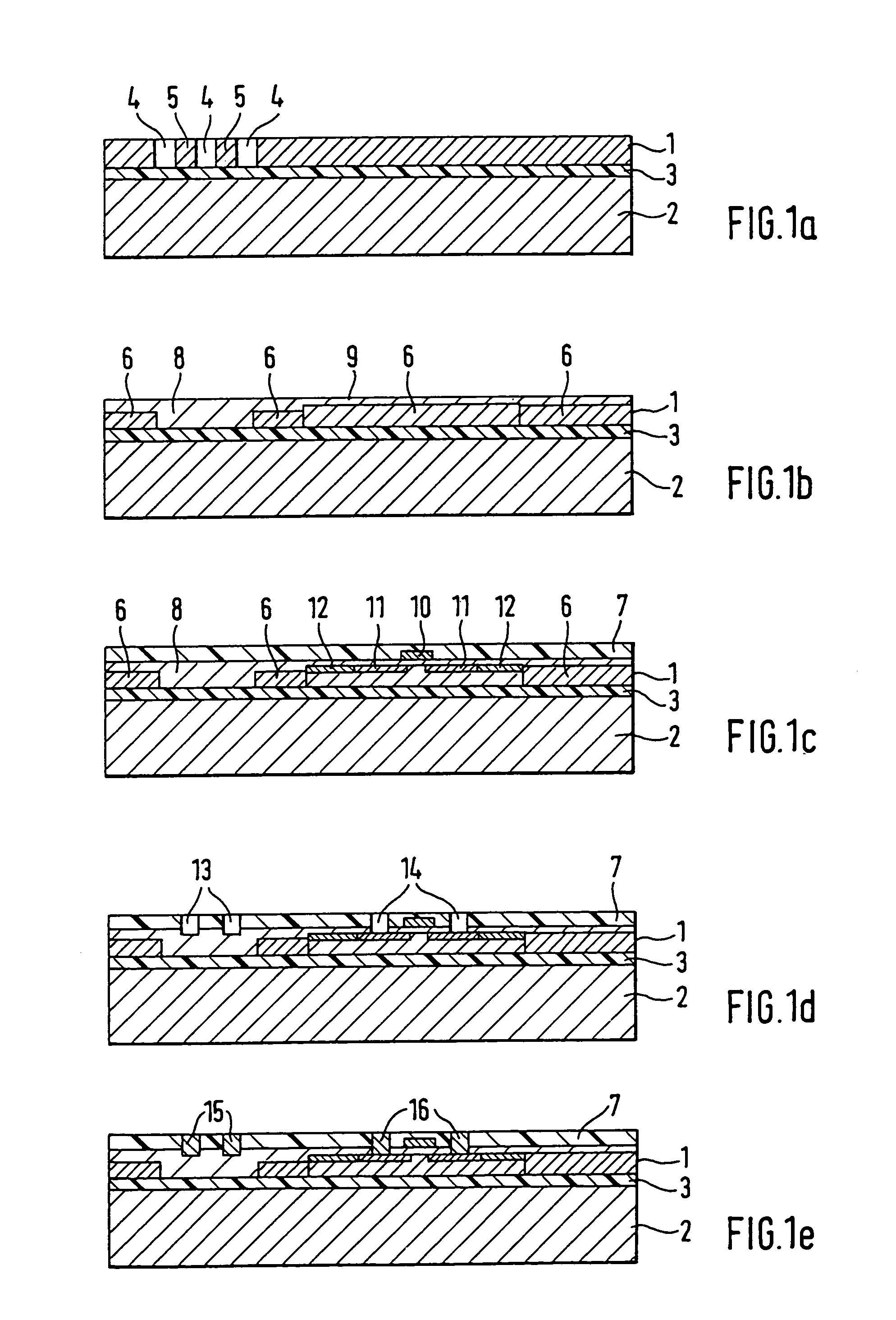
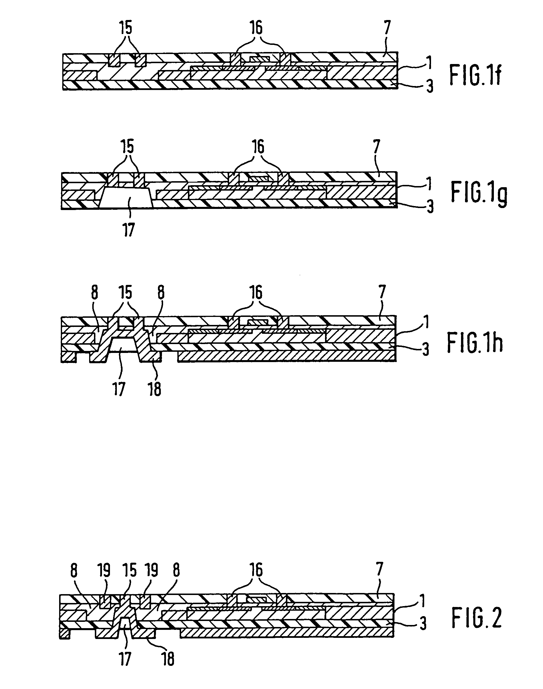
[0013]FIG. 1a shows substrate 1, 2 in which insulating layer 3 is hidden. Substrate 1, 2 can consist e.g. of silicon, insulating layer 3 e.g. of silicon dioxide. Such substrates are known and referred to as SOI (silicon on insulator) substrates. Gaps 4 are formed, e.g. by etching, in substrate 1 above insulating layer 3 as far as insulating layer 3 and surrounding bars 5 in substrate 1. Bars 5 are so dimensioned that they can be completely oxidized in a following process step. Gaps 4 and bars 5 are so dimensioned that their surface area suffices for receiving contacts for vertical integration and for forming an insulation for said contacts. Simultaneously with gaps 4, alignment marks (not shown) can also be etched to be later used for aligning the circuits or the substrate for vertical integration.

[0014]FIG. 1b shows SOI substrate 1, 2, 3 after further process steps. Differently doped tubs 6 and oxide layers 8 and 9 have been produced. Doped tubs 6 as well as field oxide 8 and gate ...


PUM


Abstract

This invention relates to a vertically integratable circuit and a method for producing same.
Unlike known methods for producing vertical electric connections, the present method uses process steps in the production of the vertically integratable circuit itself to permit vertical integration. This simplifies the sequence of production for vertically integratable circuits and thus the three-dimensional integrated circuit as a whole, thereby optimizing plant running times since process steps are saved. Because finished substrates are no longer the starting point for producing the vertical electric connections, an improved yield is moreover obtained since no process steps which could in particular change the already produced active circuit elements, such as steps with high process temperatures, are necessary any longer after production of the circuit elements.

Description

BACKGROUND OF THE INVENTION[0001]This invention relates to a vertically integratable circuit and a method for producing same.[0002]Vertically integratable circuits refer to semiconductor circuits produced by planar technology which are disposed vertically one above the other in several levels, resulting in three-dimensional circuits. The single components and circuit elements of the different levels are electrically interconnected by vertical contacts. This permits higher packing density to be attained compared to two-dimensional circuits, i.e. circuits in only one level. Vertical integration also offers advantages in terms of security since especially sensitive circuit elements can be disposed in levels or layers surrounded on both sides by at least one further level or layer with active components.[0003]In the production of the three-dimensional circuits, in particular the vertical contacts deviate from known technologies since the single vertically integratable circuits are produ...

Claims


Application Information

Patent Timeline
IPC IPC(8): H01L21/44H01L23/52H01L21/3205H01L21/60H01L21/768H01L21/98H01L25/065H01L25/07H01L25/18H01L27/00
CPCH01L21/76898H01L25/50H01L2924/0002H01L2924/00H01L21/283
Inventor GRASSL, THOMAS
Owner GIESECKE & DEVRIENT GMBH
Why Eureka
Try Eureka