Manufacturing method of semiconductor device, including differently spaced bump electrode arrays

a manufacturing method and semiconductor technology, applied in semiconductor devices, solid-state devices, basic electric elements, etc., can solve problems such as deteriorating the sealing performance of semiconductor chips, and achieve the effects of improving the sealing performance of electronic components, suppressing voids, and increasing resin injection pressur

Active Publication Date: 2006-12-05
SEIKO EPSON CORP
View PDF8 Cites 12 Cited by
  • Summary
  • Abstract
  • Description
  • Claims
  • Application Information

AI Technical Summary

Benefits of technology

[0009]Accordingly, it is possible to increase a resin injection pressure at the narrowest bump electrode array side by changing a resin injecting direction. Thus, this makes it possible to inject the resin into the interstices between the semiconductor chip and the wiring board while enabling the resin to spread around the bump electrodes even if the spacing of the bump electrode array is narrow. Consequently, this makes it possible to suppress an occurrence of a void in a sealing resin injected into the interstices between the semiconductor chip and the wiring board without increasing complex and laborious handling in manufacturing processes and also to improve a sealing performance of the semiconductor chip that is subjected to face-down mounting.
[0023]Accordingly, it is possible to increase a resin injection pressure at the most narrow bump electrode array side by changing a resin injecting direction while a resin flowing channel is shortened. As a result, it is possible to suppress an occurrence of a void in a sealing resin injected into the interstices between the electronic component and the wiring board and also to improve a sealing performance of the electronic component that is subjected to flip-chip mounting without increasing complex and laborious handling in manufacturing processes.

Problems solved by technology

Along with a miniaturization of circuit patterns, since the bump electrode is- arrayed in a fine pitch, a void occurs in the sealing resin injected into the interstices between the semiconductor chip and the film substrate which deteriorates a sealing performance of the semiconductor chip.

Method used


Image

  • Manufacturing method of semiconductor device, including differently spaced bump electrode arrays
  • Manufacturing method of semiconductor device, including differently spaced bump electrode arrays
  • Manufacturing method of semiconductor device, including differently spaced bump electrode arrays

Examples


first embodiment

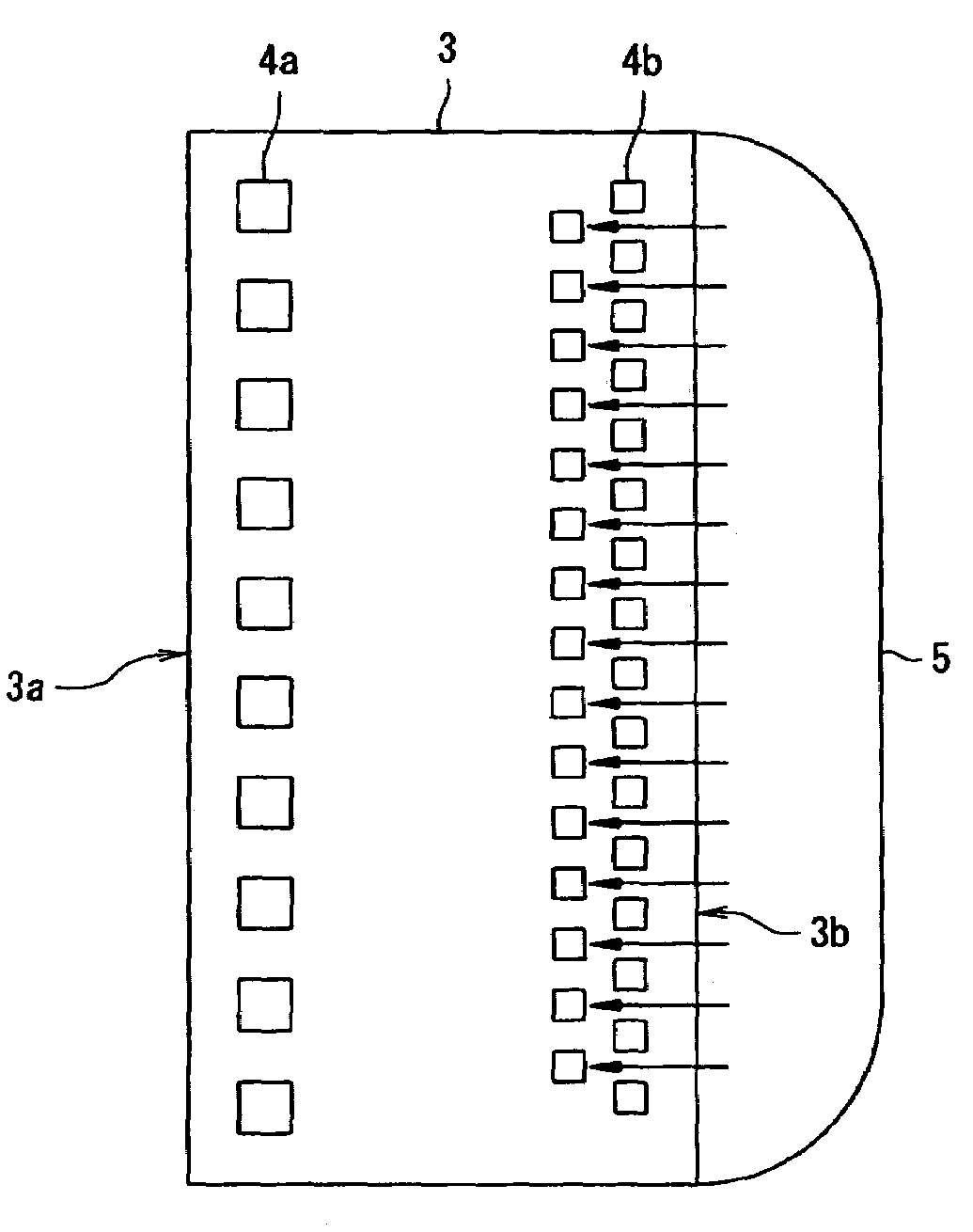
[0029]FIG. 1(a) is a sectional view showing a manufacturing method of a semiconductor device of the invention. FIG. 1(b) is a plan view showing a flow of a sealing resin 5 on a semiconductor chip 3 shown in FIG. 1(a).

[0030]In FIG. 1, a connecting terminal 2 is connected to the wiring portion 2′. Bump electrodes 4a and 4b are disposed on the semiconductor chip 3. The bump electrodes 4a are arrayed in a straight line along one long side 3a of the semiconductor chip 3 and the bump electrodes 4b are arrayed in a zigzag arrangement along the other long side 3b of the semiconductor chip 3.

[0031]The semiconductor chip 3 is subjected to face-down mounting in which the bump electrodes 4a and 4b are connected onto the wiring terminal 2. A surface of the semiconductor chip 3 is sealed by injecting the sealing resin 5 into the interstices between the semiconductor chip 3 and the film substrate 1. Here, it is possible to carry out the injection of the sealing resin 5 from the long side 3b along ...

second embodiment

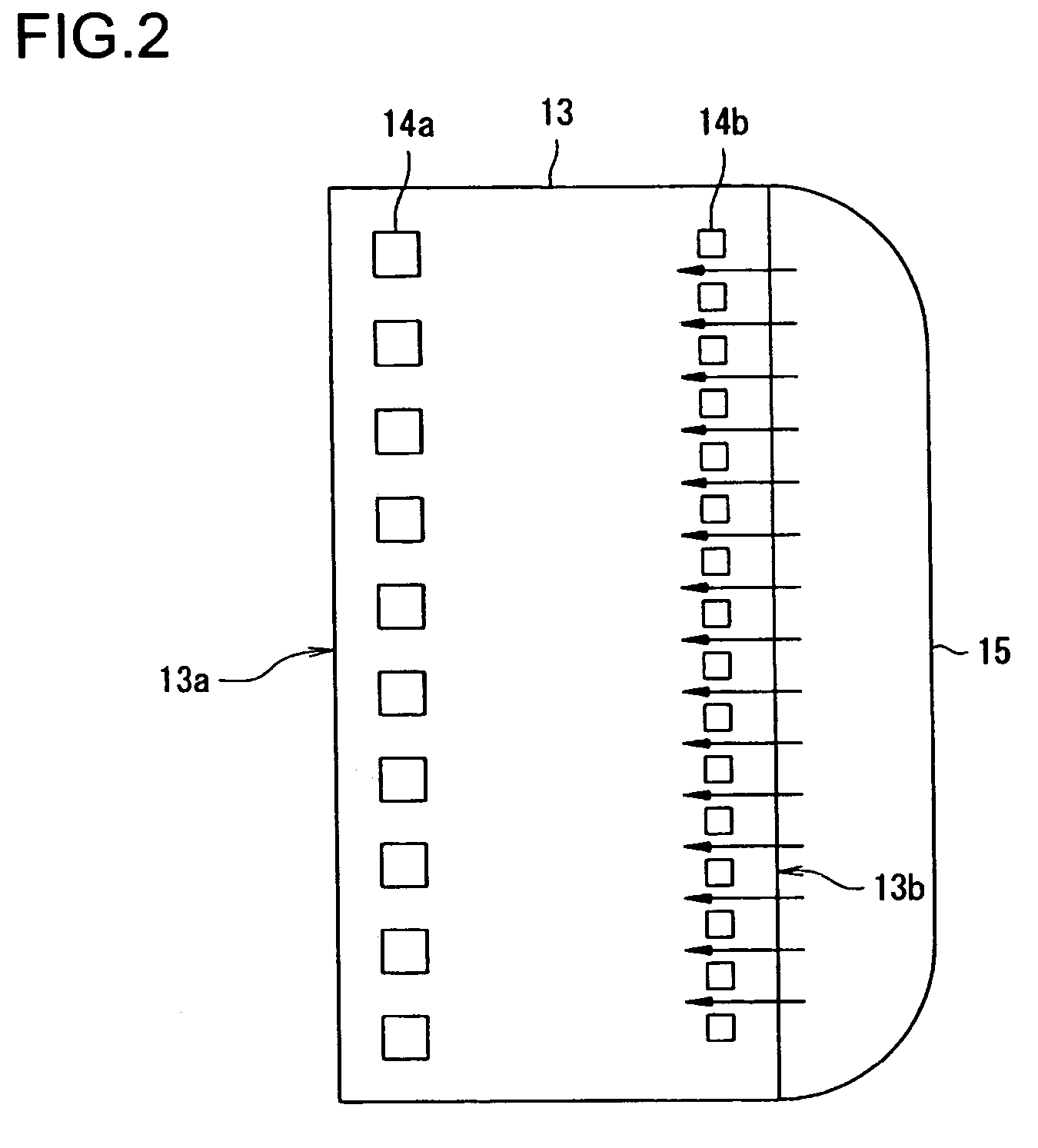
[0034]FIG. 2 is a plan view showing a flow of a sealing resin 15 on a semiconductor chip 13 of the invention.

[0035]In FIG. 2, bump electrodes 14a and 14b are disposed on the semiconductor 13. Each bump electrode array 14a and 14b is respectively arranged in a straight line along a long side 13a or 13b opposing each other on the semiconductor chip 13. A spacing between the bump electrodes 14b in the array is narrower than that of the bump electrodes 14a. Here, it is possible to carry out the injection of the sealing resin 15 from the long side 13b along which the bump electrodes 14b are arrayed to seal the surface of the semiconductor chip 13 that is subjected to face-down mounting via the bump electrodes 14a and 14b.

[0036]Accordingly, it is possible to increase an injection pressure of the sealing resin 15 at the array side of the bump electrodes 14b having a more narrow spacing than that of the bump electrodes 14a by adjusting an injecting direction of the sealing resin 15. Thus, ...

third embodiment

[0037]FIG. 3 is a plan view showing a flow of a sealing resin 25 on the semiconductor chip 23 of the invention.

[0038]In FIG. 3, bump electrodes 24a and 24b are disposed on the semiconductor chip 23. Here, the bump electrodes 24a are arrayed in a straight line along one long side 23a of the semiconductor chip 23 and the bump electrodes 24b are arrayed in a straight line along the other long side 23b and each short side 23c and 23d of the semiconductor chip 23. A spacing between the bump electrodes 24b in the array is narrower than that of the bump electrodes 24a. Here, it is possible to carry out the injection of the sealing resin 25 from the long side 23b along which the bump electrodes 24b are arrayed to seal the surface of the semiconductor chip 23 that is subjected to face-down mounting via the bump electrodes 24a and 24b.

[0039]Accordingly, it is possible to increase an injection pressure of the sealing resin 25 at the array side of the bump electrodes 24b having a more narrow s...


PUM


Abstract

First bump electrodes are arrayed in a straight line along a first side of a semiconductor chip. Second bump electrodes are more narrowly arrayed in a zigzag arrangement along a second side of the chip. By carrying out an injection of a sealing resin from the second side on which the second bump electrodes are arrayed, a surface of the semiconductor chip that is subjected to face-down mounting on a film substrate is sealed.

Description

RELATED APPLICATIONS[0001]This application claims priority to Japanese Patent Application No. 2003-142323 filed May 20, 2003 which is hereby expressly incorporated by reference herein in its entirety.BACKGROUND[0002]1. Field of the Invention[0003]The present invention relates to a manufacturing method of a semiconductor device and a manufacturing method of an electronic device, especially adequate for resin sealing processes such as COF (Chip On Film).[0004]2. Description of the Related Art[0005]As for a conventional semiconductor device, for example, as disclosed in Japanese Unexamined Patent Application Publication No. 2000-269611, a method that a semiconductor is flip-chip mounted on a film substrate by bonding of a bump electrode on a connecting terminal formed on the film substrate is introduced. As for a method to seal the semiconductor chip that is flip-chip mounted, a sealing resin is injected into the interstices between the semiconductor chip and the film substrate.[0006]A...

Claims


Application Information

Patent Timeline
Patent Type & Authority Patents(United States)
IPC IPC(8): H01L21/44H01L21/48H01L21/50H01L21/60H01L21/56H01L23/485
CPCH01L21/563H01L24/06H01L24/13H01L24/10H01L24/28H01L2224/0401H01L2224/73204H01L2224/32225H01L2224/16225H01L2924/01033H01L2924/01082H01L2924/0105H01L2924/01049H01L2924/01006H01L2224/06153H01L2224/13099H01L2224/73203H01L2224/83102H01L2224/92125H01L2924/01004H01L2924/01005H01L2924/00012H01L2924/00H01L2224/13
Inventor YUZAWA, HIDEKI
Owner SEIKO EPSON CORP
Why Eureka
Try Eureka