MEMS RF switch

a technology of rf switch and rf switch, which is applied in the direction of solid-state devices, semiconductor devices, relays, etc., can solve the problem of high aspect ratio devices

Active Publication Date: 2006-12-05
US SEC THE AIR FORCE THE
View PDF15 Cites 96 Cited by
  • Summary
  • Abstract
  • Description
  • Claims
  • Application Information

AI Technical Summary

Benefits of technology

[0033]It is another object of the invention to provide a MEMS switch enclosure process in which internal pressur

Problems solved by technology

These arrangements involve low temperature processes and may result in a high aspe

Method used


Image

  • MEMS RF switch
  • MEMS RF switch
  • MEMS RF switch

Examples


Embodiment Construction

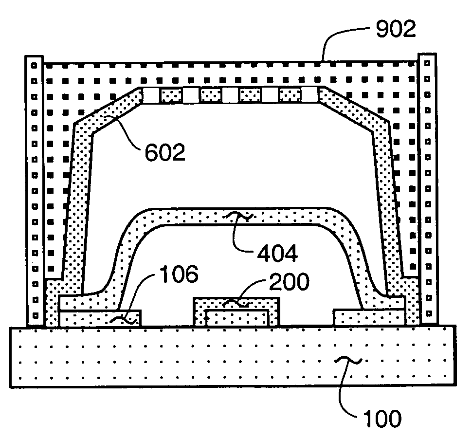
[0062]The following detailed description of the invention is divided according to the major steps in fabricating a MEMS radio frequency switch device according to the invention. These major steps are generally identified as switch metal fabrication, dielectric switch encapsulation and switch sealing using a liquid or gaseous phase sequence Notwithstanding a division into these major steps in the description, this process at least through FIG. 6, may be viewed as a unitary sequence with the processing step headings disregarded. Alternatives and other details appear in the drawings subsequent to FIG. 6. The process described herein accomplishes a capacitance operated MEMS switch; the process is however equally relevant to a metal contact switch.

RF Metal Process

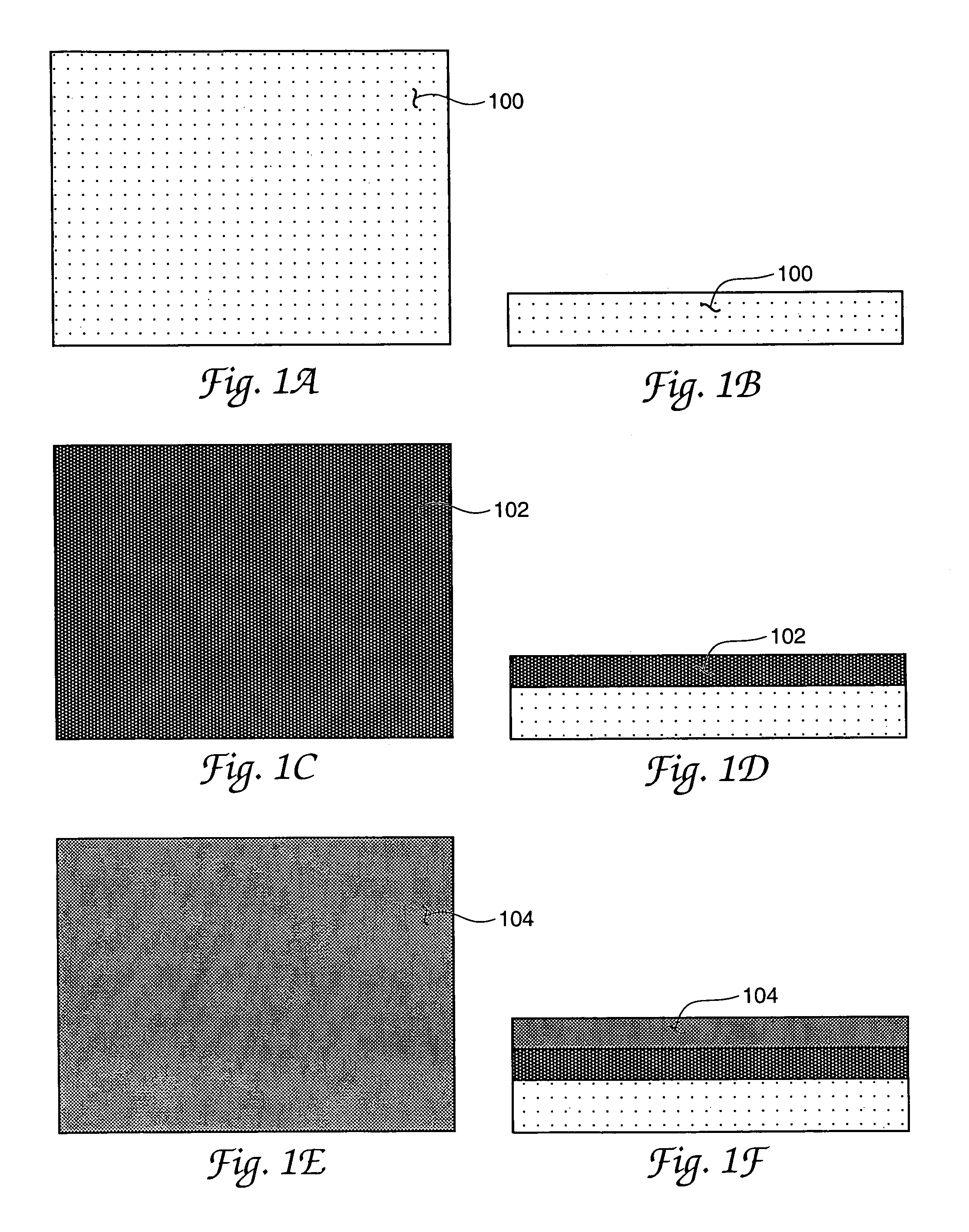
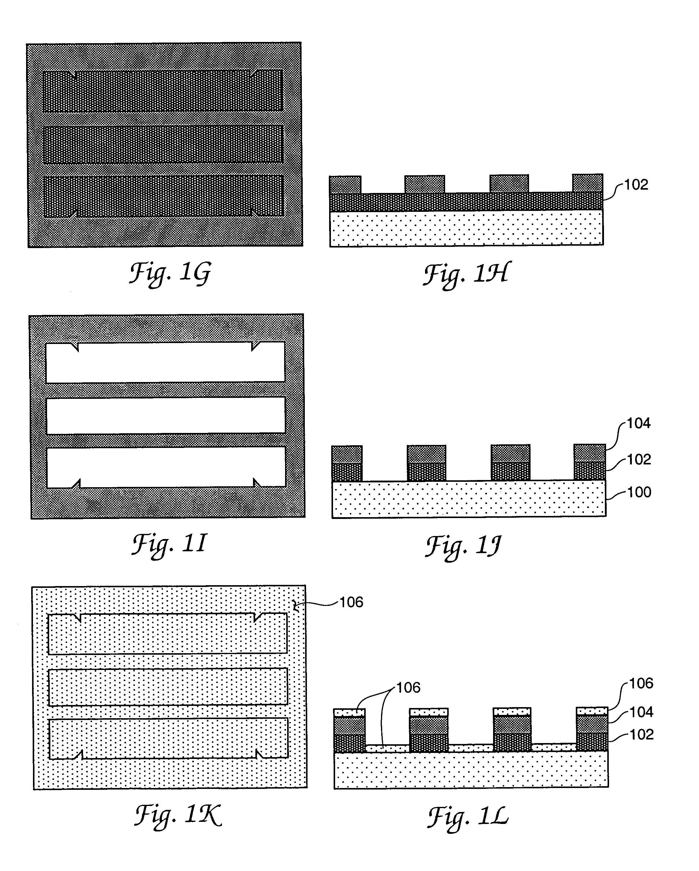
[0063]RF metal defines the bottom contact in a capacitive switch arrangement according to the invention. The metal thickness used determines the power handling capability of the switch. High power switches require thick metal (g...


PUM


Abstract

A capacitance coupled, transmission line-fed, radio frequency MEMS switch and its fabrication process using photoresist and other low temperature processing steps are described. The achieved switch is disposed in a low cost dielectric housing free of undesired electrical effects on the switch and on the transmission line(s) coupling the switch to an electrical circuit. The dielectric housing is provided with an array of sealable apertures useful for wet, but hydrofluoric acid-free, removal of switch fabrication employed materials and also useful during processing for controlling the operating atmosphere surrounding the switch—e.g. at a pressure above the high vacuum level for enhanced switch damping during operation. Alternative arrangements for sealing an array of dielectric housing apertures are included. Processing details including plan and profile drawing views, specific equipment and materials identifications, temperatures and times are also disclosed.

Description

CLAIM OF PRIORITY[0001]This application claims the benefit of U.S. Provisional Application No. 60 / 573,892 filed May 24, 2004. The contents of this provisional application are hereby incorporated by reference herein.RIGHTS OF THE GOVERNMENT[0002]The invention described herein may be manufactured and used by or for the Government of the United States for all governmental purposes without the payment of any royalty.CROSS REFERENCE TO RELATED PATENT DOCUMENT[0003]The present document is related to the copending and commonly assigned patent application document “MEMS RF SWITCH INTEGRATED PROCESS”, AFD 685, Ser. No. 10 / 901,315 filed of even date herewith. The contents of this related even filing date document are hereby incorporated by reference herein.BACKGROUND OF THE INVENTION[0004]MEMS technology has numerous applications in both commercial and military electrical systems. MEMS switches, for instance, can be used in routing radio frequency and microwave frequency signals in high frequ...

Claims


Application Information

Patent Timeline
IPC IPC(8): H01L21/14
CPCH01H59/0009
Inventor EBEL, JOHN L.CORTEZ, REBECCASTRAWSER, RICHARD E.LEEDY, KEVIN D.
Owner US SEC THE AIR FORCE THE
Why Eureka
Try Eureka