Differential comparator, analog/digital conversion apparatus and imaging apparatus

a technology of analog/digital conversion and comparator, applied in the field ofdifferential comparator, analog/digital conversion apparatus and imaging apparatus, can solve the problems of pixel level, pixel noise, and degrade the accuracy of analog/digital conversion, so as to improve the digitalization accuracy of analog signals based on relevant comparisons, increase parasitic capacitance, and suppress consumption current

Inactive Publication Date: 2006-12-05
SOCIONEXT INC
View PDF10 Cites 28 Cited by
  • Summary
  • Abstract
  • Description
  • Claims
  • Application Information

AI Technical Summary

Benefits of technology

[0020]It is an object of the present invention to provide a differential comparator capable of realizing highly accurate analog / digital conversion with the lesser amount of consumption current.
[0021]It is another object of the present invention to provide an analog / digital converter apparatus capable of realizing highly accurate analog / digital conversion with the lesser amount of consumption current.
[0022]It is another object of the present invention to provide an imaging apparatus capable of outputting high quality picture data with the lesser amount of consumption current.

Problems solved by technology

However, its fixed pattern noise due to the unevenness in a characteristic among amplifiers at each pixel level is a problem.
However, any of the above-mentioned technologies of Patent References 1 through 4 does not recognize the following technical problems caused when the comparator of the analog / digital converter is composed of only an inverter, or an inverter and a differential amplifier.
Therefore, if the reference voltage is inputted for comparison, the potential at a point A, point B attempts to transit to the potential of the amount of charge stored in C100 based on the potential at point A. However, since there is the parasitic capacitor C200, point B changes at a ratio between C100 and C200, and the accuracy of analog / digital conversion degrades, which is a technical problem.
In a configuration using an inverter, the consumption current of the inverter is high.
More particularly, in a configuration where a lot of ADC is provided for each column, like column ADC in the CMOS image sensor, the total consumption current of the imaging device becomes very high.

Method used


Image

  • Differential comparator, analog/digital conversion apparatus and imaging apparatus
  • Differential comparator, analog/digital conversion apparatus and imaging apparatus
  • Differential comparator, analog/digital conversion apparatus and imaging apparatus

Examples


Embodiment Construction

[0039]The preferred embodiment of the present invention is described below with reference to the drawings.

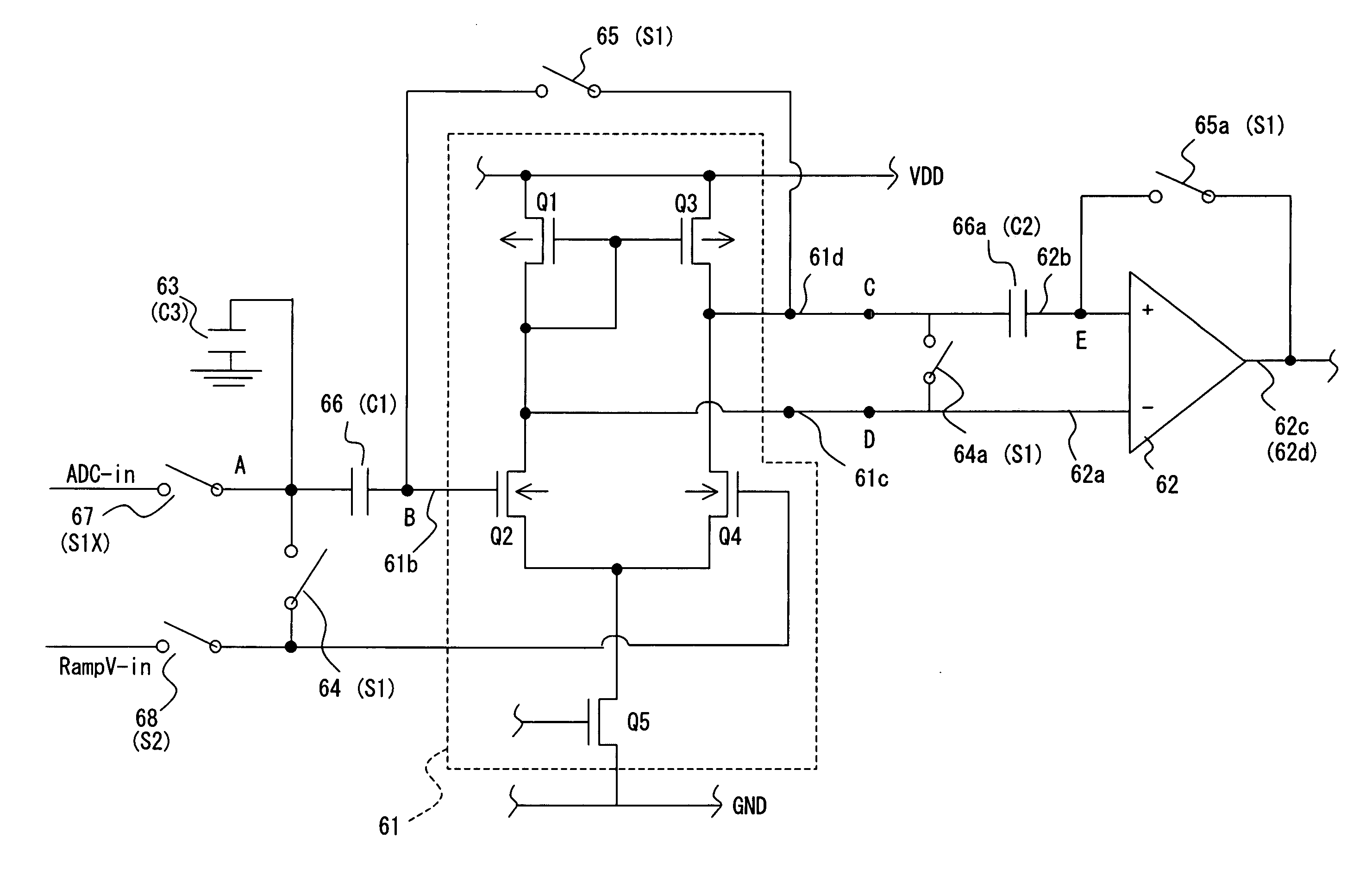
[0040]FIG. 3 is a block diagram showing one configuration of an analog / digital converter apparatus including the differential comparator which is one preferred embodiment of the present invention. FIG. 4 is a circuit diagram showing in detail its internal configuration. FIG. 5 is a block diagram showing one entire configuration of an imaging apparatus including the analog / digital converter apparatus which is one preferred embodiment of the present invention.

[0041]The preferred embodiment is described using a case where the present invention is applied to an imaging apparatus 10 composed of, for example, a CMOS image sensor.

[0042]As shown in FIG. 5, the imaging apparatus 10 in this preferred embodiment comprises a pixel array 20 in which a plurality of pixel units 23 are two-dimensionally arrayed along each row 21 and each column 22, a vertical scan circuit 31 and a horizontal sc...


PUM


Abstract

A differential comparator which outputs positive and / or negative logic signals to an output terminal according to the coincidence / non-coincidence of first and second input signal levels inputted to first and second input terminals, respectively, comprises an offset cancel function composed of an offset capacitor device provided on the differential comparator side of the first and second terminals, a first switch for short-circuiting the first and second input terminals in such a way as to form a closed loop including the offset capacitor device, and a second switch for short-circuiting both the connection point between the offset capacitor device and the differential comparator, and the output terminal.

Description

CROSS-REFERENCE TO RELATED APPLICATIONS[0001]This application is based upon and claims the benefit of priority from Japanese Patent Application No. 2004-197329, filed in Jul. 2, 2004, the entire contents of which are incorporated herein by reference.BACKGROUND OF THE INVENTION[0002]1. Field of the Invention[0003]The present invention relates to a differential comparator, an analog / digital conversion apparatus and an imaging apparatus, more particularly, to a technology effective when applied to the reading circuit of optical / electrical conversion signals in a complementary metal oxide semiconductor (CMOS) image sensor and the like.[0004]2. Description of the Related Art[0005]Attention is paid to a CMOS image sensor, for example, for the reason that the CMOS image sensor matches the manufacturing process, operating voltage and the like in surrounding image processing circuits, and that an imaging apparatus, an image processing circuit, a controller and the like can be easily integrat...

Claims


Application Information

Patent Timeline
Patent Type & Authority Patents(United States)
IPC IPC(8): H03M1/12H03K5/08H03M1/08H03M1/10H03M1/38H04N5/335H04N5/365H04N5/374H04N5/378
CPCH03M1/0607H04N5/335H04N25/00H04N25/67H04N25/75
Inventor MIZUGUCHI, TOSHITAKAFUNAKOSHI, JUNYAMAGATA, SEIJIHIGUCHI, TSUYOSHI
Owner SOCIONEXT INC
Why Eureka
Try Eureka