Method for time-domain synchronization across a bit-sliced data path design

a data path and time-domain technology, applied in the direction of digital transmission, generating/distributing signals, instruments, etc., can solve problems such as data corruption

Active Publication Date: 2006-12-12
RIBBON COMM OPERATING CO INC
View PDF15 Cites 17 Cited by
  • Summary
  • Abstract
  • Description
  • Claims
  • Application Information

AI Technical Summary

Problems solved by technology

Multiple chips are used to operate on a large data bus that is too wide to fit into a single chip because a single chip cannot handle the processing of data for the entire data bus.
A problem is introduced if the data has to synchronously cross a time domain across all data slices.
A problem is introduced because the signal should cross from the first time domain to the second time domain in all slices at the same time.
If the signal does not cross a time domain in all chip slices at the same time, data corruption may result.
Thus, the signal may arrive at the second time domain for the two chips at different times. Then, the two chips may not be processing data on the same clock cycle, which may result in errors.

Method used


Image

  • Method for time-domain synchronization across a bit-sliced data path design
  • Method for time-domain synchronization across a bit-sliced data path design
  • Method for time-domain synchronization across a bit-sliced data path design

Examples


Embodiment Construction

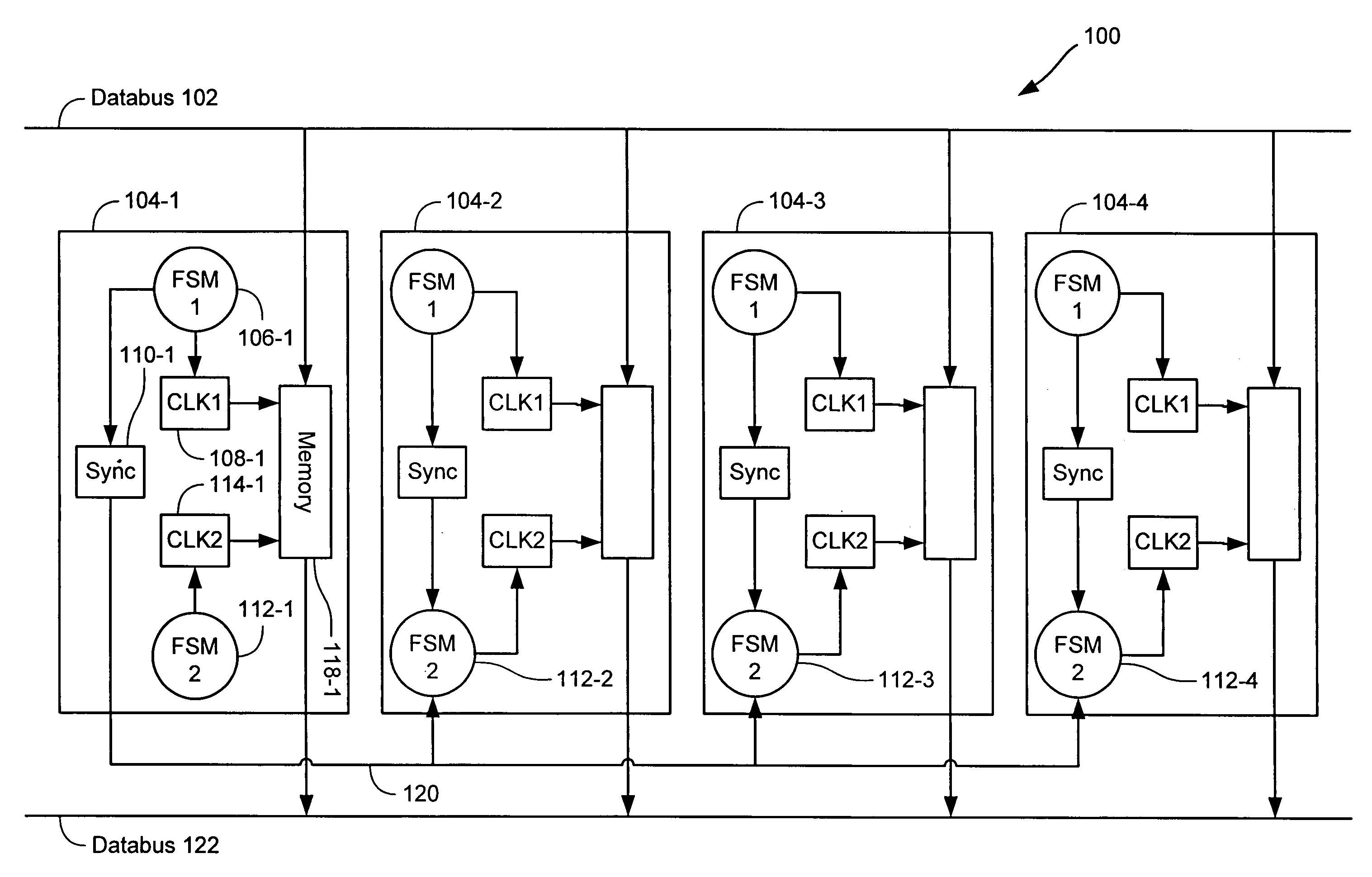
[0016]FIG. 1 depicts a bit slice data path design 100 according to one embodiment of the present invention. As shown, a data bus 102, a data bus 122, and a plurality of chips 104 are provided. The plurality of chips are depicted as a master chip 104-1 and a plurality of slave chips 104-2, 104-3, and 104-4. Although four chips are shown, it will be understood that any number of chips may be included in bit slice data path design 100.

[0017]In one embodiment, each chip 104 in system 100 is designed with substantially the same circuitry. Although it will be described that each chip 104 includes the same circuitry, it will be understood that variations in the circuitry may exist. However, it will be recognized that the chips in a bit slice design are designed to process data for a slice of the data bus on the same clock cycle.

[0018]Master chip 104-1 includes a first time domain that includes a finite state machine 106-1 and a clock (CLK1) 108-1. A synchronization circuit 110-1 is used to...


PUM


Abstract

A bit slice data path design is provided. Multiple chips are coupled to a data bus and configured to process a slice of data for the data bus. One chip in the design is designated as a master chip and the other chips are designated as slaves. A master chip sends a signal from a first time domain to a second time domain through a synchronization circuit. When the signal has been synchronized to the frequency of the second time domain, the signal is sent to the slave chips through a connection. The signal is also looped back to the second time domain in the master chip so that the signal reaches the second time domain in the master and slave chips in the same clock cycle.

Description

CROSS-REFERENCES TO RELATED APPLICATIONS[0001]This application claims priority to U.S. Provisional Application No. 60 / 455,490, filed Mar. 17, 2003, which is incorporated herein by reference for all purposes.BACKGROUND OF THE INVENTION[0002]The present invention generally relates to a bit slice data path design and more specifically to techniques for synchronizing signals that cross two different time domains for chips in a bit slice data path design.[0003]The bit slice data path design includes multiple chips that are coupled to a common data bus. The multiple chips are used to process a slice of data for the data bus. Multiple chips are used to operate on a large data bus that is too wide to fit into a single chip because a single chip cannot handle the processing of data for the entire data bus.[0004]Each of the multiple chips process data on the same clock-for-clock cycle. A problem is introduced if the data has to synchronously cross a time domain across all data slices. For exa...

Claims


Application Information

Patent Timeline
Patent Type & Authority Patents(United States)
IPC IPC(8): G06F1/12
CPCH04L7/0008H04L7/02
Inventor MARINO, JOHN
Owner RIBBON COMM OPERATING CO INC
Why Eureka
Try Eureka