Display device with reduced deterioration of emission layer

Inactive Publication Date: 2006-12-19
SANYO ELECTRIC CO LTD
View PDF15 Cites 0 Cited by
  • Summary
  • Abstract
  • Description
  • Claims
  • Application Information

AI Technical Summary

Benefits of technology

[0012]An object of the present invention is to provide a display capable of preventing an emission layer (organic layer) from deterioration resulting from temperature rise of an electrode

Problems solved by technology

In this case, the current concentrates to the outlet terminal 104 of the cathode 103, disadvantageously leading to resistance heating of the outlet terminal 104.
Even if the width of a single outlet terminal part is increased, however, large current concentrically flows to the single outlet terminal part when the display is increased in size, and hence it is difficult to reduce the quantity of heat generation in the outlet terminal part.
When the display is increased in size, therefore, it is so difficult to reduce temperature rise of a cathode that it is also difficult to prevent organic layer

Method used


Image

  • Display device with reduced deterioration of emission layer
  • Display device with reduced deterioration of emission layer
  • Display device with reduced deterioration of emission layer

Examples


Example

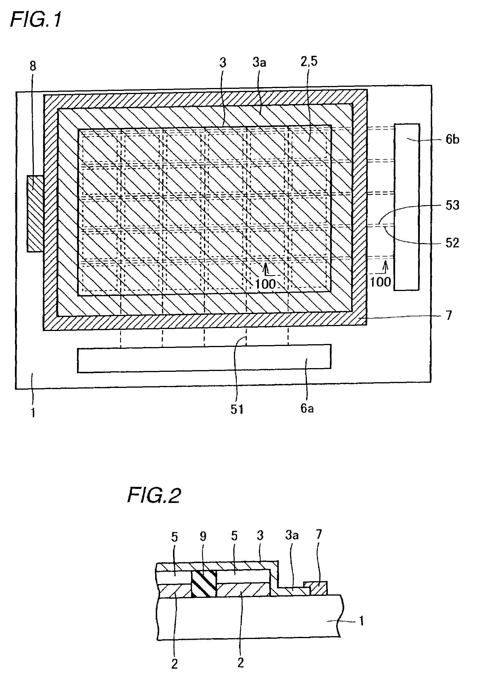
[0041](First Embodiment)

[0042]Referring to FIGS. 1 and 2, anodes 2 consisting of transparent metal oxide films of ITO (indium-tin oxide) or the like having a thickness of about 100 nm are formed on a glass substrate 1 in an organic EL display according to a first embodiment of the present invention. Organic layers 5 are formed on the anodes 2. The organic layers 5 consist of hole injection layers formed on the anodes 2, hole transport layers formed on the hole injection layers and emission layers formed on the hole transport layers. A cathode 3 consisting of a low work function material such as MgIn having a thickness of about 300 nm is formed on the organic layers 5 to cover the overall structure.

[0043]The glass substrate 1 is an example of the “substrate” according to the present invention. The anodes 2 are examples of the “first electrode” according to the present invention, and the cathode 3 is an example of the “second electrode” according to the present invention. The organic ...

Example

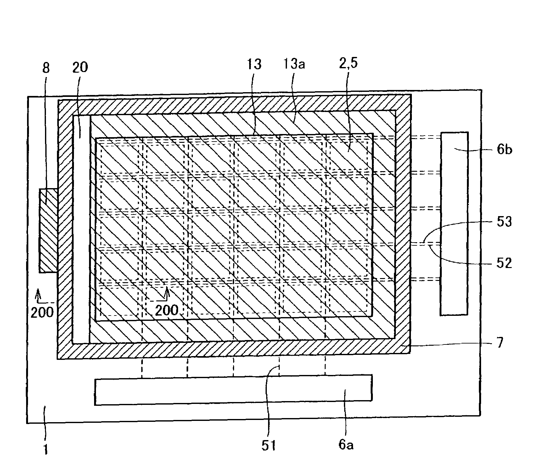
[0049](Second Embodiment)

[0050]Referring to FIGS. 3 to 5, an opening 20 is provided between an edge of a peripheral electrode 7 connected with a current supply terminal 8 and a corresponding edge of a cathode 13 in an organic EL display according to a second embodiment of the present invention while mounting a cooling fin 14 on the current supply terminal 8 in a structure similar to that of the first embodiment shown in FIG. 1. The remaining structure of the organic EL display according to the second embodiment is similar to that of the aforementioned organic EL display according to the first embodiment. The organic EL display according to the second embodiment is now described in detail.

[0051]In the organic EL display according to the second embodiment, anodes 2 of ITO or the like are formed on a glass substrate 1, similarly to the aforementioned first embodiment. Organic layers 5 consisting of hole injection layers, hole transport layers and emission layers in ascending order are ...

Example

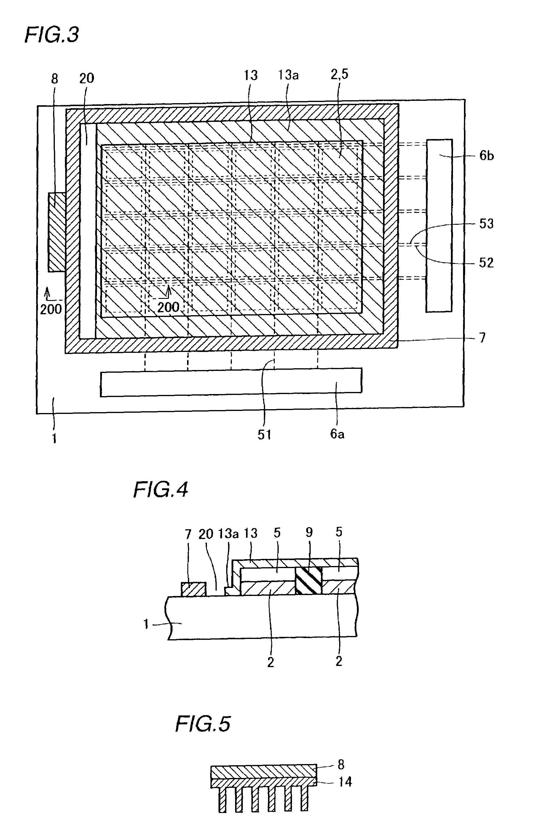
[0058](Third Embodiment)

[0059]Referring to FIGS. 6 and 7, a cathode 23 and a peripheral electrode 7 are totally in contact with each other on three edges of the cathode 23 while one edge of the cathode 23 is connected to the peripheral electrode 7 through a plurality of outlet terminals 23b in an organic EL display according to a third embodiment of the present invention. The remaining structure of the organic EL display according to the third embodiment is similar to that of the aforementioned organic EL display according to the first embodiment.

[0060]According to the third embodiment, an edge of the cathode 23 corresponding to an edge of the peripheral electrode 7 connected with a current supply input terminal 8 is irregularly formed for forming the plurality of outlet terminals 23b by projecting portions of the irregular shape. The edge of the peripheral electrode 7 connected with the current supply input terminal 8 is connected with one edge of the cathode 23 through the plurali...


PUM


Abstract

A display capable of preventing an emission layer from deterioration resulting from temperature rise of an electrode also when the same is increased in size and easily connectable with an external current source also when the same is connected with the external current source on a single portion is provided. This display comprises a first electrode formed on a substrate, an emission layer formed on the first electrode, a second electrode formed on the emission layer, a peripheral electrode, arranged to enclose the outer periphery of the second electrode and connected with at least three edges of the outer periphery of the second electrode, having a smaller sheet resistance value than the second electrode, and a current source connection terminal connected to the outer periphery of the peripheral electrode. Thus, current readily flows from the second electrode toward the peripheral electrode, while the current can be dispersedly fed along three or four directions.

Description

BACKGROUND OF THE INVENTION[0001]1. Field of the Invention[0002]The present invention relates to a display, and more specifically, it relates to a display including an emission layer such as an organic layer.[0003]2. Description of the Background Art[0004]Requirement for flat display devices exhibiting smaller power consumption than a generally employed CRT is recently increased following diversification of information apparatuses. Among such flat display devices, a display employing an organic electroluminescence element (hereinafter referred to as an organic EL element) characterized by high efficiency, thinness / lightweight property and no view angle dependency is actively researched and developed.[0005]FIG. 12 is a perspective view showing the overall structure of a conventional organic EL display. FIG. 13 is a plan view of the conventional organic EL display shown in FIG. 12. Referring to FIGS. 12 and 13, anodes 102 of ITO (indium-tin oxide) are formed on a glass substrate 101 i...

Claims


Application Information

Patent Timeline
IPC IPC(8): H05B33/02H05B33/06G09F9/00G09F9/30H01L27/32H01L51/50H01L51/52H05B33/26
CPCH01L27/3244H01L51/5228H01L51/529H10K59/12H10K50/824H10K50/87
Inventor HAMADA, YUJITSUJIOKA, TSUYOSHIMATSUSUE, NORIYUKI
Owner SANYO ELECTRIC CO LTD
Why Eureka
Try Eureka