
Dual channel source measurement unit for semiconductor device testing

a measurement unit and semiconductor technology, applied in the direction of measurement devices, electronic circuit testing, instruments, etc., can solve the problems of limiting the output power available to each dut, requiring the same voltage potential for all connected duts, and imposing penalties on certain types of testing

Active Publication Date: 2006-12-19
QUALITAU
View PDF7 Cites 6 Cited by
  • Summary
  • Abstract
  • Description
  • Claims
  • Application Information

AI Technical Summary

Benefits of technology

"The invention is a dual channel source measurement unit (SMU) that separates the stress and monitor parts of the unit, allowing for optimal performance of each. This means that the SMU can source different voltages to different devices under test (DUTs) simultaneously, which is useful in situations where the time between stress and monitor phases needs to be minimized. The technical effect of this invention is improved performance and efficiency in testing multiple DUTs simultaneously."

Problems solved by technology

While the Single Channel Multiple Output SMU configuration does allow multiple DUTs to be tested using a single SMU, it has limitations that impose penalties on certain types of testing.
One of the main limitations is the requirement of all connected DUTs to have the same voltage potential applied.
This limitation is imposed by having a single programmable voltage source, which all the buffered sources follow.
Another limitation is that the output power available to each DUT is restricted to that of the buffered sources.
Practically, this means the stress and monitor phase of a test are limited to the same power conditions.

Method used


Image

  • Dual channel source measurement unit for semiconductor device testing
  • Dual channel source measurement unit for semiconductor device testing
  • Dual channel source measurement unit for semiconductor device testing

Examples


Embodiment Construction

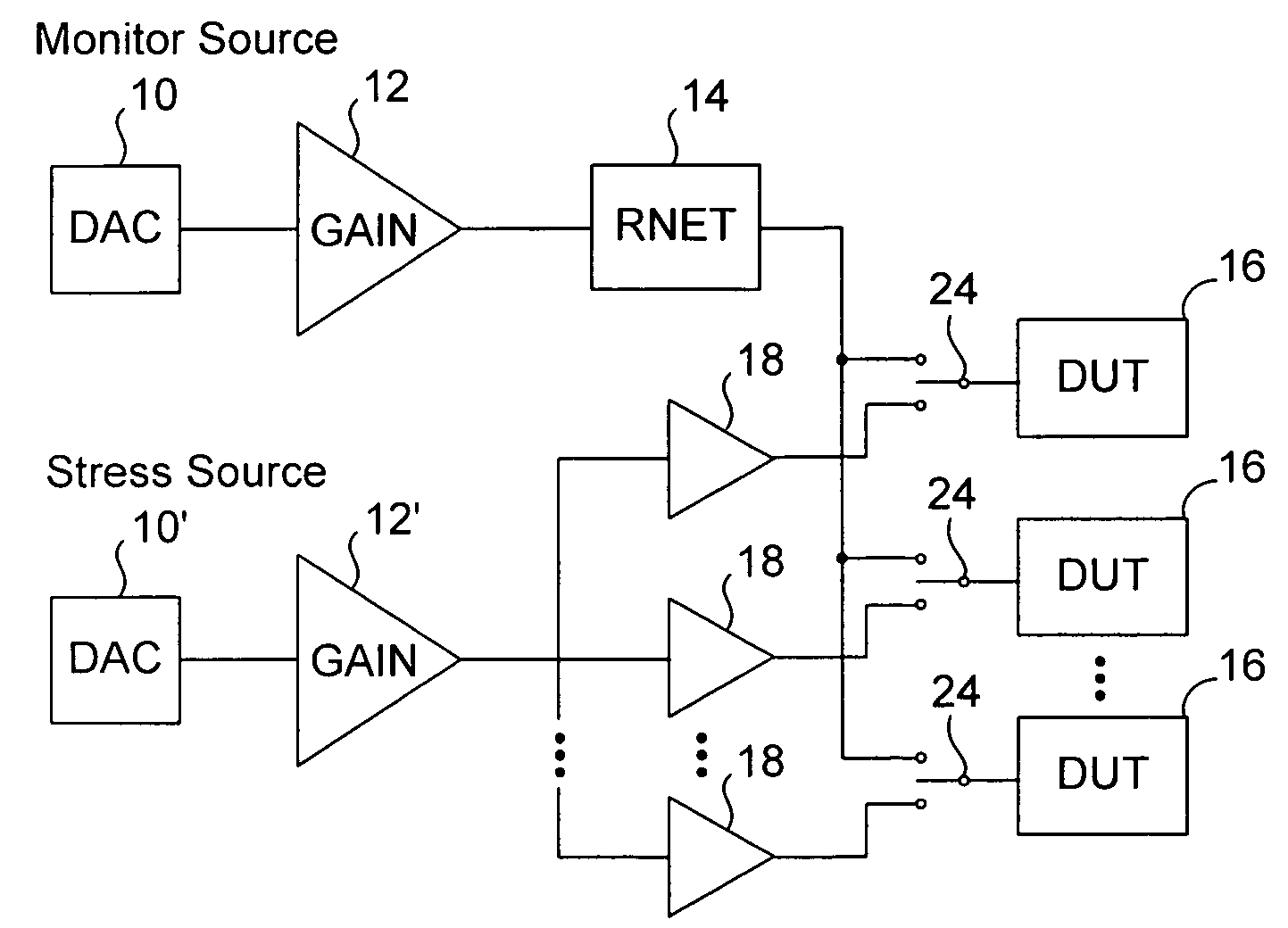
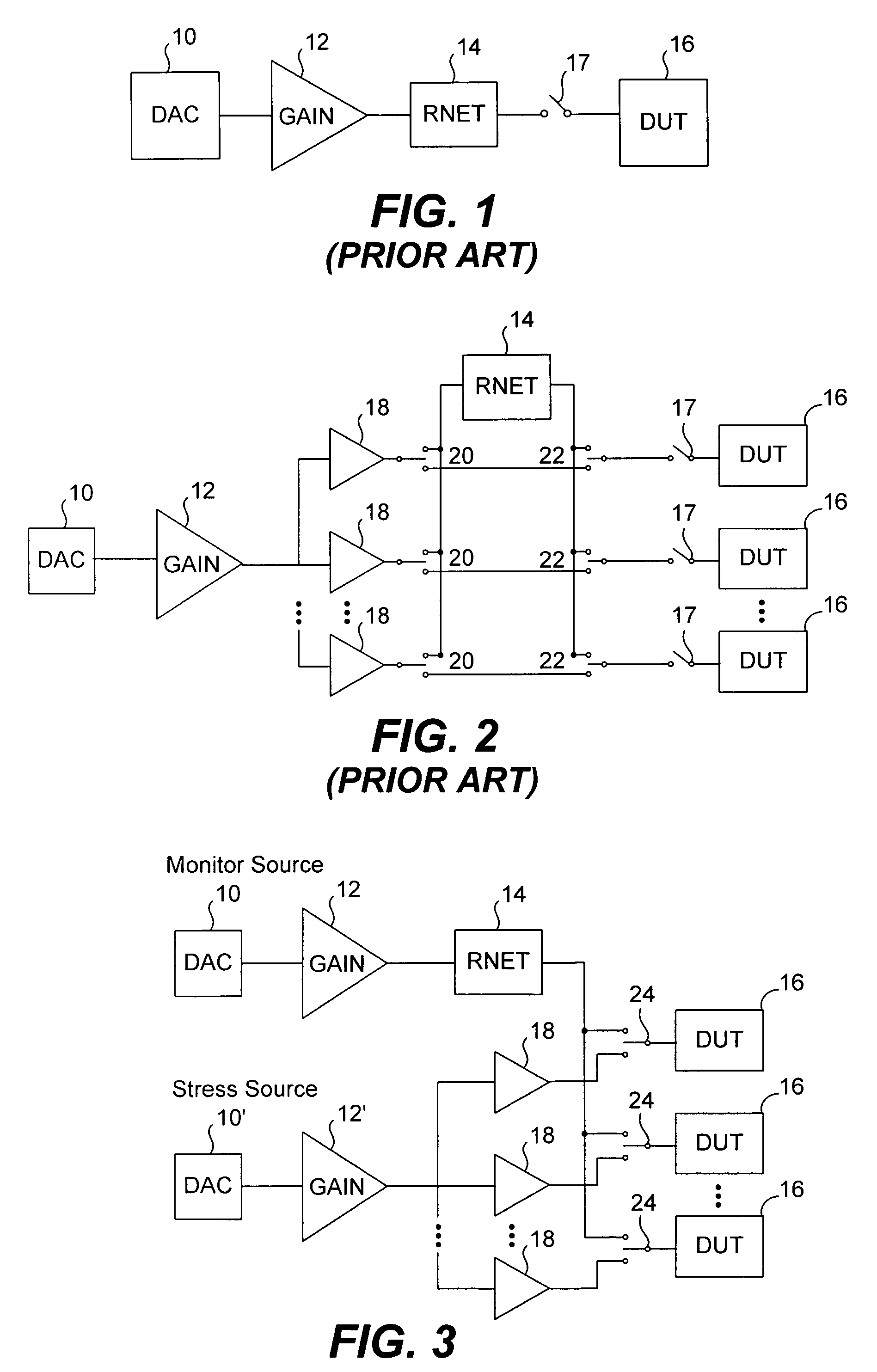
[0015]As noted above, the source measurement unit has two programmable voltage sources which are referred to as the stress source and the monitor source. While the stress source has no other function than outputting a set voltage, the monitor voltage and its connected circuitry provide several other capabilities including measuring current flowing through the source, source and current while measuring the output voltage at the source, and the capability to limit either voltage or current to a programmed compliance level. Along with the stress and monitor sources, the SMU has several voltage following buffers each of which can be connected to the device under test (DUT). The buffers are configured so that they follow the output of the stress source, and their outputs can be switched so that the monitor source makes connection with the DUT.

[0016]FIG. 3 is a functional block diagram of a dual channel SMU in accordance with an embodiment of the invention which decouples the stress and m...


PUM


Abstract

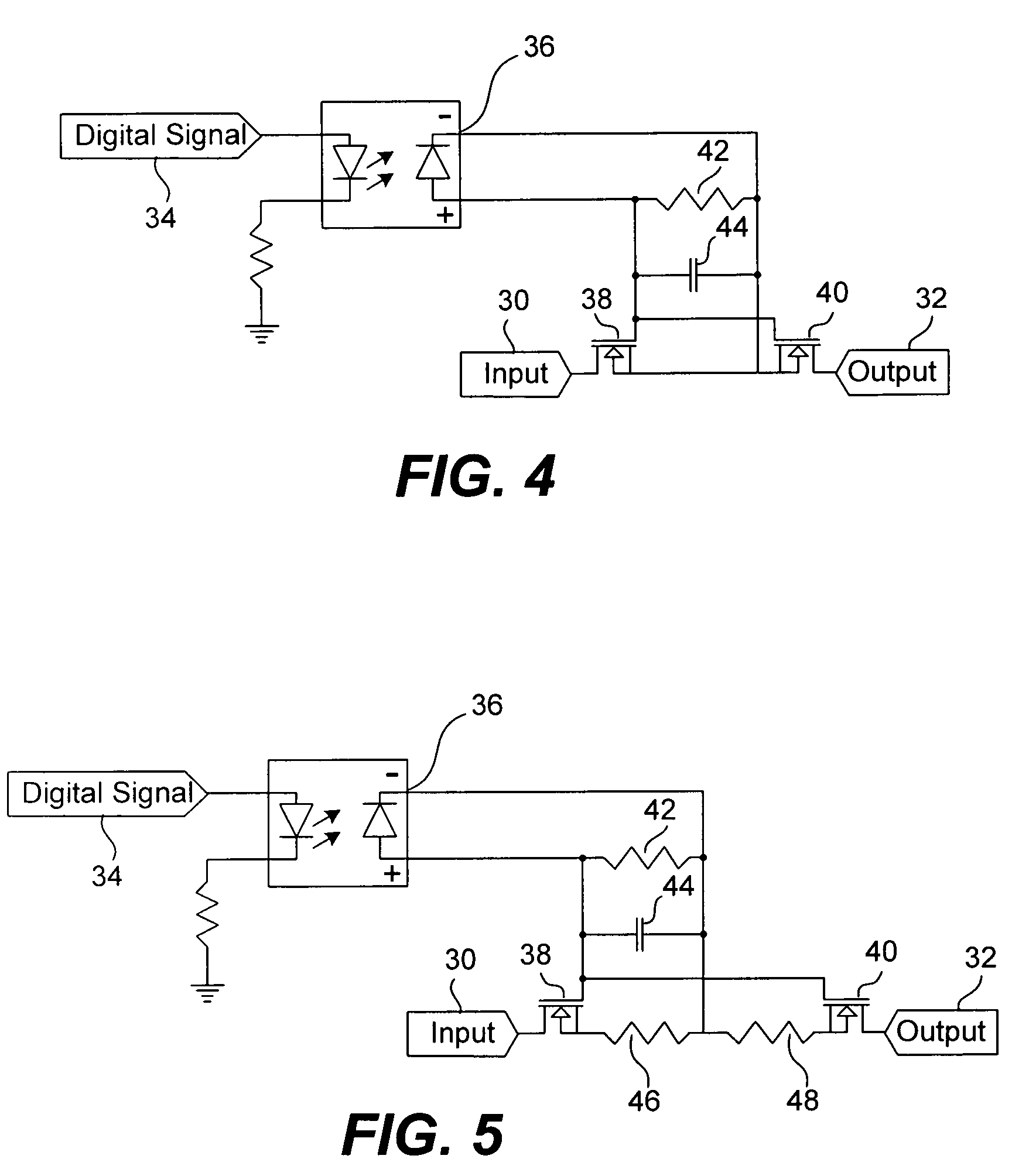
A dual channel source measurement unit for reliability testing of electrical devices provides a voltage stress stimulus to a device under test and monitors degradation to the device under test caused by the stress simulator. The dual channel source measurement unit decouples the stress and monitor portions of the unit so that the requirements of each can be optimized. Deglitching and current clamp switches can be incorporated in the dual channel source measurement unit to prevent glitches in the switching circuitry and to limit or clamp current flow to or from the monitor and stress sources.

Description

CROSS REFERENCE TO RELATED APPLICATIONS[0001]This application claims priority to U.S. Provisional Patent Application No. 60 / 550,380, filed Mar. 5, 2004, which is incorporated herein for all purposes.BACKGROUND OF THE INVENTION[0002]This invention relates generally to semiconductor device testing, and more particularly the invention relates to a dual channel source measurement unit (SMU) for testing semiconductor device reliability.[0003]A SMU as used for semiconductor reliability testing provides a voltage stress stimulus to a device under test (DUT) and monitors degradation to the DUT caused by the stress stimulus. FIG. 1 is a block diagram of a SMU which includes a digital to analog converter (DAC) 10, gain or amplification block 12, and a resistor network or RNET 14 for measuring current flow to or from the DUT16 through switch 17. The voltage source DAC 10 and gain unit 12 provide the stress stimulus to DUT 16, while RNET 14 provides monitoring capabilities.[0004]A semiconductor...

Claims


Application Information

Patent Timeline
Patent Type & Authority Patents(United States)
IPC IPC(8): G01R31/26G01R1/00G01R31/00G01R31/319
CPCG01R31/31926
Inventor RAICHMAN, TALCUEVAS, PETER P.BORTHWICK, JAMESCASOLO, MICHAEL A.
Owner QUALITAU
Learn More