Circuit and method for a switch matrix and switch sensing

a switch matrix and circuit technology, applied in the field of switch matrix, can solve the problems of increasing requiring significant processor resources, and adding considerable accumulative costs, so as to reduce the number of i/o linens, reduce the number of i/o lines going to the processor, and reduce the cost

Inactive Publication Date: 2006-12-19
IMMERSION CORPORATION
View PDF79 Cites 88 Cited by
  • Summary
  • Abstract
  • Description
  • Claims
  • Application Information

AI Technical Summary

Benefits of technology

[0008]Through the present invention, a more efficient and lower cost switch matrix circuit is provided. In one embodiment, the present invention senses current instead of voltage to detect open or closed switches, where resistors and a transistor are used for each column of the matrix to provide selection signals to a processor to determine which button(s) of the matrix have been pressed. In addition, the number of I / O lines going to the processor can be reduced by utilizing bi-directional scan lines and scanning only one switch at a time instead of an entire row of switches at a time. A further embodiment that is a variation on the current sensing matrix can use an analog-to-digital converter to sense the switch states, but, likewise, uses the bi-directional scan lines to reduce the number of I / O linens going to the processor. These and other advantages will become readily apparent from the following detailed description and accompanying drawings.

Problems solved by technology

While the conventional switch matrix can provide switch selection indication and avoid ghosting, the conventional approach is input / output (I / O) intensive, requiring significant processor resources in providing scan line processing.
The conventional switch matrix further requires one diode per switch to prevent ghosting, which adds considerable accumulative cost as the number of switches within a matrix grows.

Method used


Image

  • Circuit and method for a switch matrix and switch sensing
  • Circuit and method for a switch matrix and switch sensing
  • Circuit and method for a switch matrix and switch sensing

Examples


Embodiment Construction

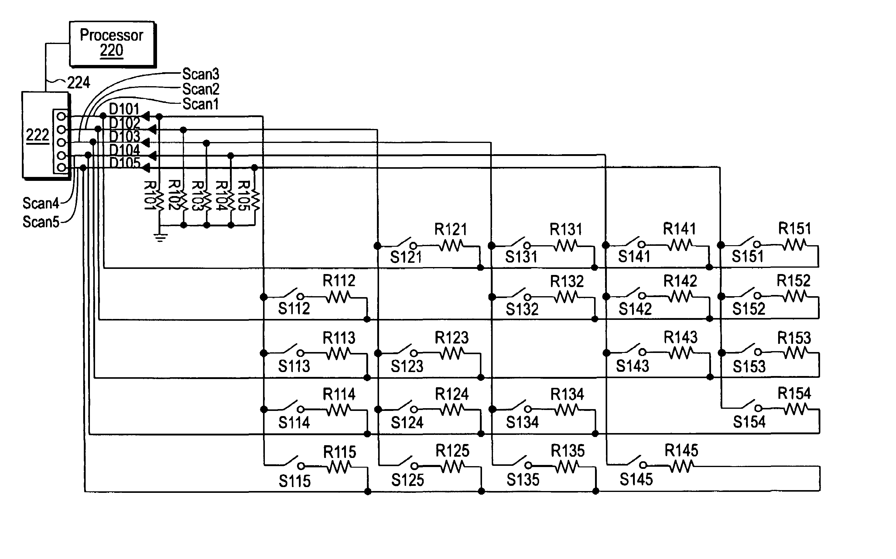
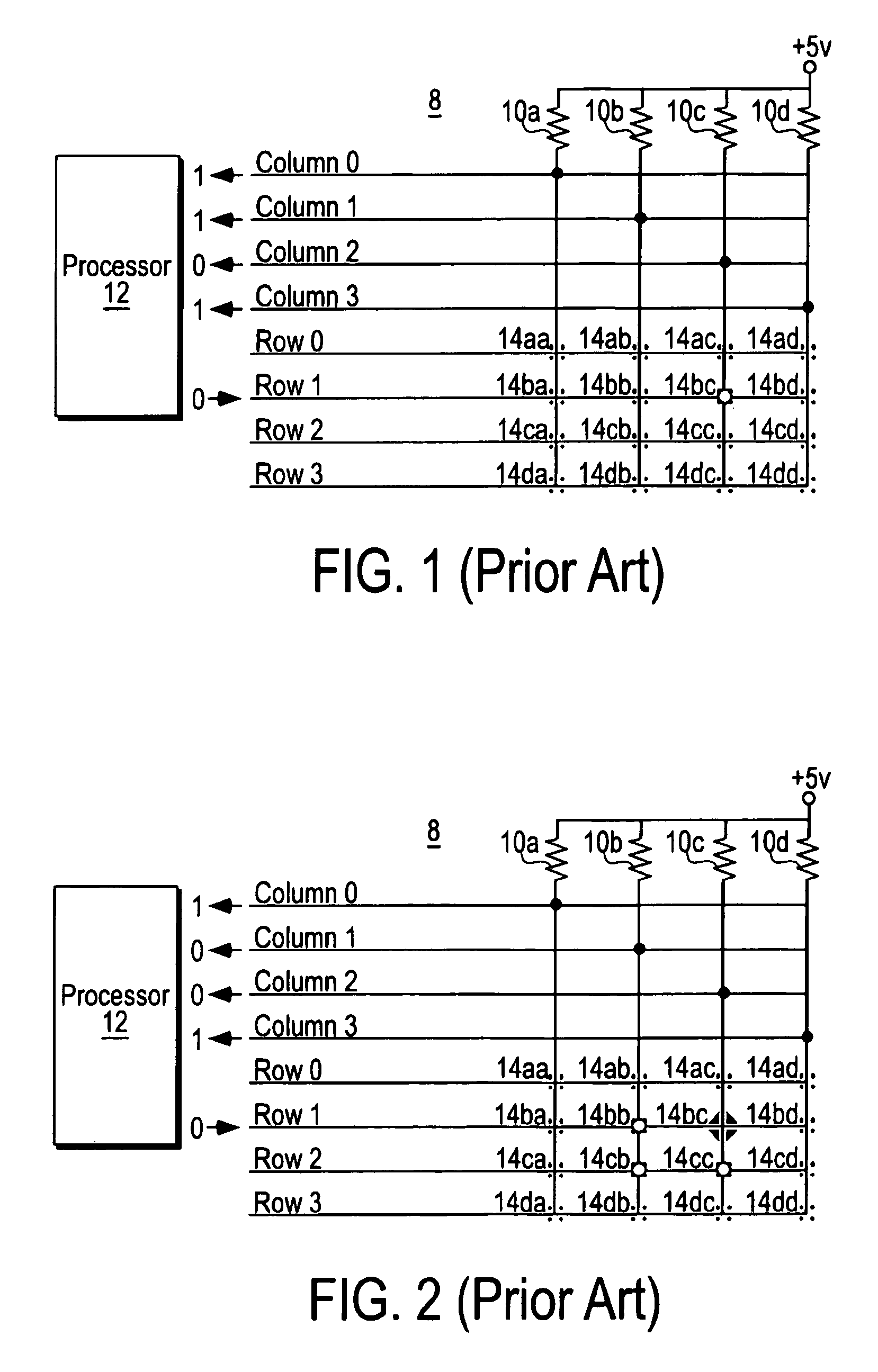
[0016]The present invention relates to a switch matrix circuit. The following description is presented to enable one of ordinary skill in the art to make and use the invention and is provided in the context of a patent application and its requirements. Various modifications to the preferred embodiment and the generic principles and features described herein will be readily apparent to those skilled in the art. Thus, the present invention is not intended to be limited to the embodiment shown but is to be accorded the widest scope consistent with the principles and features described herein.

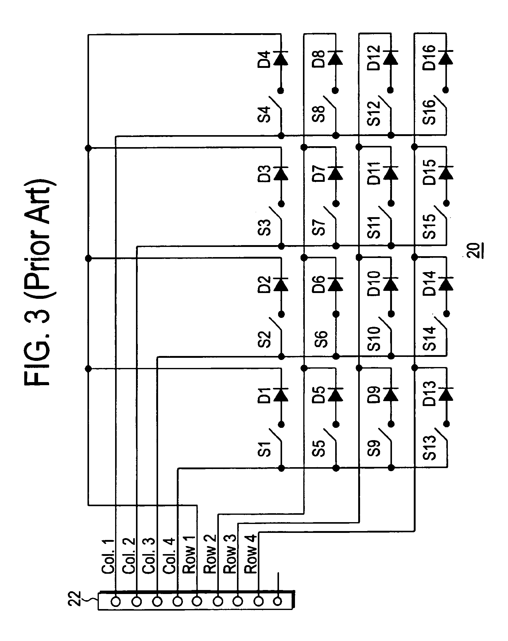
[0017]FIG. 4 illustrates a schematic of a current sensing switch matrix 100 in accordance with one embodiment of the present invention. As indicated by its name, the detection of a closed switch in the matrix is based on current. Similar to the conventional matrix, only one of the rows is driven low at a time. In the example of FIG. 4, 16 switches, S1′ through S16′, are included and each is coupled...


PUM


Abstract

Aspects of a switch matrix circuit are provided. In accordance with a circuit aspect, a plurality of switches are organized in a row and column configuration. Coupled to the plurality of switches is a current sensing circuit. The current sensing circuit includes a transistor and at least one resistor per column of the plurality of switches. Current amplified by the transistor and converted by the at least one resistor in a column is sensed as a logic level indicative of a switch status within the column for a selected row. The current sensing arrangement may also be used in an embodiment utilizing bi-directional signal control to minimize the number of I / O lines required to scan the switch matrix. The bi-directional signal scanning may also be implemented in another embodiment that senses voltage levels to determine switch closures.

Description

FIELD OF THE INVENTION[0001]The present invention relates to a switch matrix, and more particularly to an efficient, low cost switch matrix.BACKGROUND OF THE INVENTION[0002]In various interface devices, such as keypads, joysticks, wheels, gamepads, etc., detection of user selections of differing buttons and switches is needed. A standard switch matrix operates like a grid of horizontal and vertical conductors. At all points where the horizontal and vertical conductors cross, a switch is located. Pressing / closing the switch connects the two conductors. FIG. 1 presents a functional diagram of a standard matrix 8 of sixteen (16) switches, a 4×4 matrix. In the standard 16 switch matrix, four of the conductors or row lines, Row 0, Row 1, Row 2, and Row 3, are dedicated to drive a voltage corresponding to a logic level zero into the matrix. Only one of the four rows is driven low at a time, and the remaining rows are passively pulled high by the pull-up resistors 10a, 10b, 10c, or 10d on ...

Claims


Application Information

Patent Timeline
Patent Type & Authority Patents(United States)
IPC IPC(8): H03K17/00H03K17/62H03M11/20
CPCH03M11/20H03K17/00H03M11/00
Inventor TIERLING, KOLLIN
Owner IMMERSION CORPORATION
Why Eureka
Try Eureka