Architecture for programmable logic device

a logic device and logic circuit technology, applied in the field of programmable logic device architecture, can solve the problems of inability to provide functionality that requires any additional logic circuit elements, inability to use logic circuit elements in some plbs, and limited use of logic circuit elements in other plbs, and achieve the effect of efficient utilization of logic circuit elements

Inactive Publication Date: 2006-12-26
HD SILICON SOLUTIONS LLC
View PDF8 Cites 76 Cited by
  • Summary
  • Abstract
  • Description
  • Claims
  • Application Information

AI Technical Summary

Benefits of technology

[0006]An embodiment of the invention overcomes the above-mentioned drawbacks and provide

Problems solved by technology

A PLB is incapable of providing functionality that requires any additional logic circuit elements.
In several applications, logic circuit elements in some PLBs remain unutilized or underutilized while other PLBs are limited by the availability of insufficient quantities of logic-circuit elements.
This situation results in inefficien

Method used


Image

  • Architecture for programmable logic device
  • Architecture for programmable logic device
  • Architecture for programmable logic device

Examples


Embodiment Construction

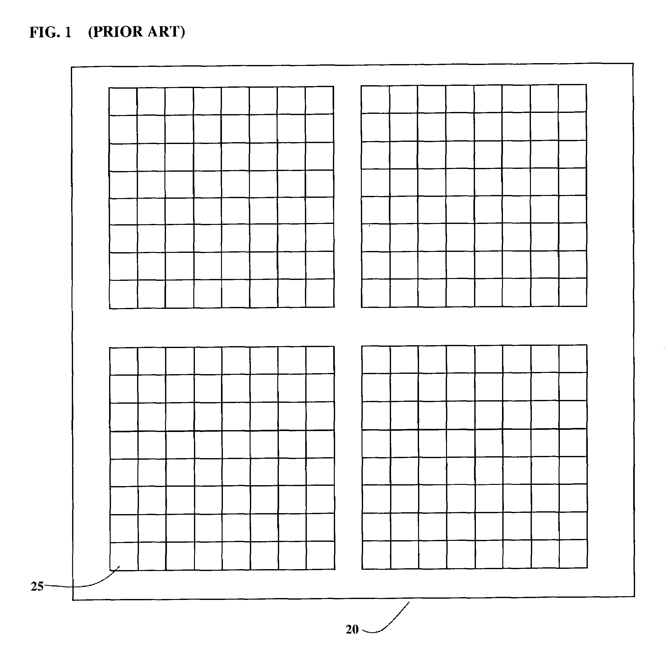
[0023]As shown in FIG. 1, a conventional FPGA 20 generally consists of an array of tiles 25 that collectively provide configurable logic-circuit element resources. The tiles 25 are programmatically interconnected to provide the desired set of functions using the resources available in one or more tiles 25.

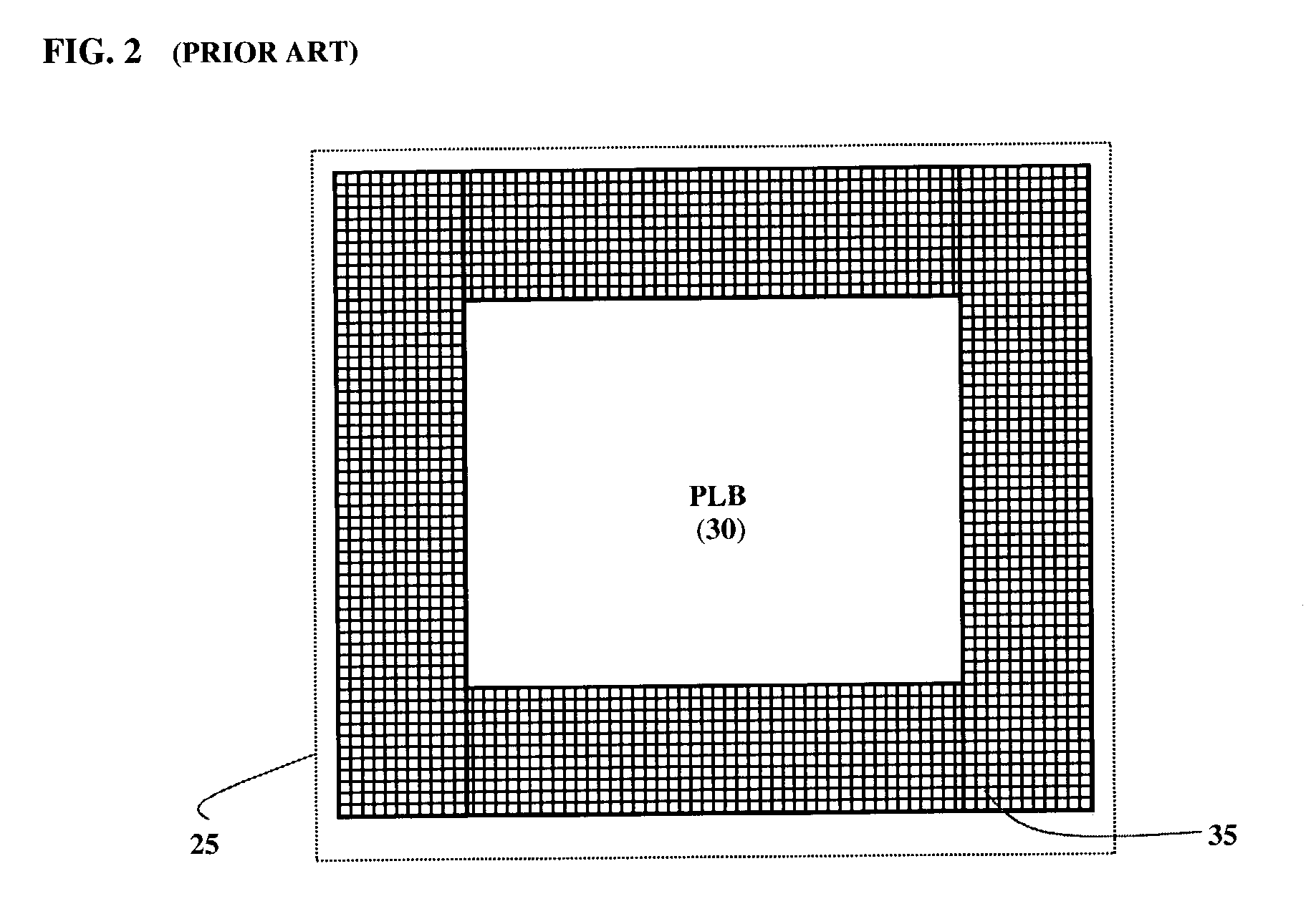
[0024]FIG. 2 shows the internal structure of a conventional tile 25. Each tile 25 is made up of a programmable logic block (PLB) 30 and routing resources 35 that connect its input and output signals with other PLBs (not shown). A PLB 30 is also termed a Configurable Logic Block (CLB), a Configurable Logic Element (CLE) or a Programmable Function Unit (PFU). A PLB 30 typically includes the circuitry in which logic can be implemented in programmable logic devices.

[0025]The interconnection between tiles 25 in existing FPGA architectures is shown in FIG. 3. A PLB 30 in one tile 25 is connected with PLBs in other tiles 25 using routing resources in the form of a Connection Bloc (CB) 40 ...


PUM


Abstract

An improved Programmable Logic Device architecture that provides more efficient utilization of resources by enabling access to defined circuit elements in the domain of any Programmable Logic Block (PLB) from any other PLB in the device, by incorporating a connecting means in the routing structure for selectively connecting the input or output of the circuit element in the domain of the PLB to the common interconnect matrix connecting all the PLBs together.

Description

PRIORITY CLAIM[0001]This application claims priority from Indian patent application No. 432 / Del2002, filed Apr. 5, 2002, which is incorporated herein by reference.FIELD OF THE INVENTION[0002]This invention relates generally to an improved programmable logic device architecture, and more particularly to an improved Field Programmable Gate Array (FPGA) architecture that provides more efficient utilization of resources by enabling access to circuit elements in the domain of one Programmable Logic Block (PLB) from other PLBs.BACKGROUND OF THE INVENTION[0003]Field Programmable Gate Arrays (FPGAs) are general-purpose logic devices that can be configured to provide any desired logic function within the range of capabilities of the FPGA. Each FPGA comprises, internally, one or more Programmable Logic Blocks (PLBs) that can be interconnected at their outputs and inputs through a programmable interconnection matrix. Each PLB includes logic-circuit elements that can be programmed to interconne...

Claims


Application Information

Patent Timeline
IPC IPC(8): H03K19/177
CPCH03K19/17736
Inventor SWAMI, PARVESHKHANNA, NAMERITAAGARWAL, DEEPAK
Owner HD SILICON SOLUTIONS LLC
Why Eureka
Try Eureka