Semiconductor integrated circuit device

a technology of integrated circuits and semiconductors, applied in information storage, static storage, digital storage, etc., can solve the problems of ensuring a write time and the inability to solve the drawbacks of phase-change memory operation, and achieve stable operation, short operation cycle time, and high-integration and high-speed nonvolatile memory

Inactive Publication Date: 2006-12-26
LONGITUDE SEMICON S A R L
View PDF3 Cites 35 Cited by
  • Summary
  • Abstract
  • Description
  • Claims
  • Application Information

AI Technical Summary

Benefits of technology

[0014]The object of the present invention is to provide a technique, which can stabilize the operation of the phase-change memory for a short operation cycle time and achieve a high-integrated and high-speed nonvolatile memory.
[0015]Another object of the present invention is to provide a technique, which can prevent a decrease of data reliability, which is caused by a change in characteristics of phase-change elements when the high-speed operation is achieved.

Problems solved by technology

That is, in the phase-change memory, there is the problem of ensuring a write time.
Thus, there is the problem that drawbacks on the operation of the phase-change memory cannot be solved only by substituting a general DRAM memory cell with a memory cell array employing the phase-change resistance.

Method used


Image

  • Semiconductor integrated circuit device
  • Semiconductor integrated circuit device
  • Semiconductor integrated circuit device

Examples


first embodiment

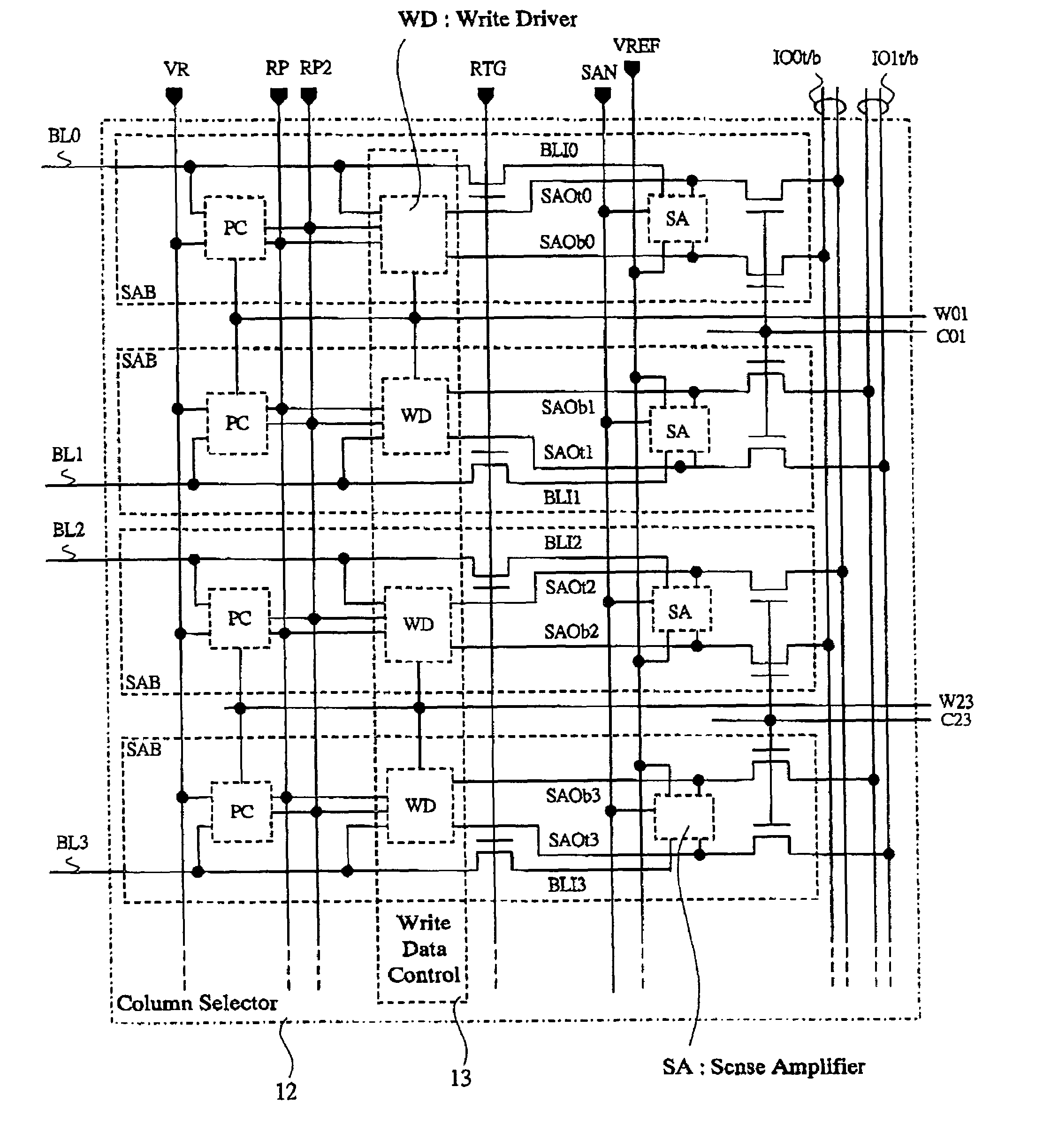
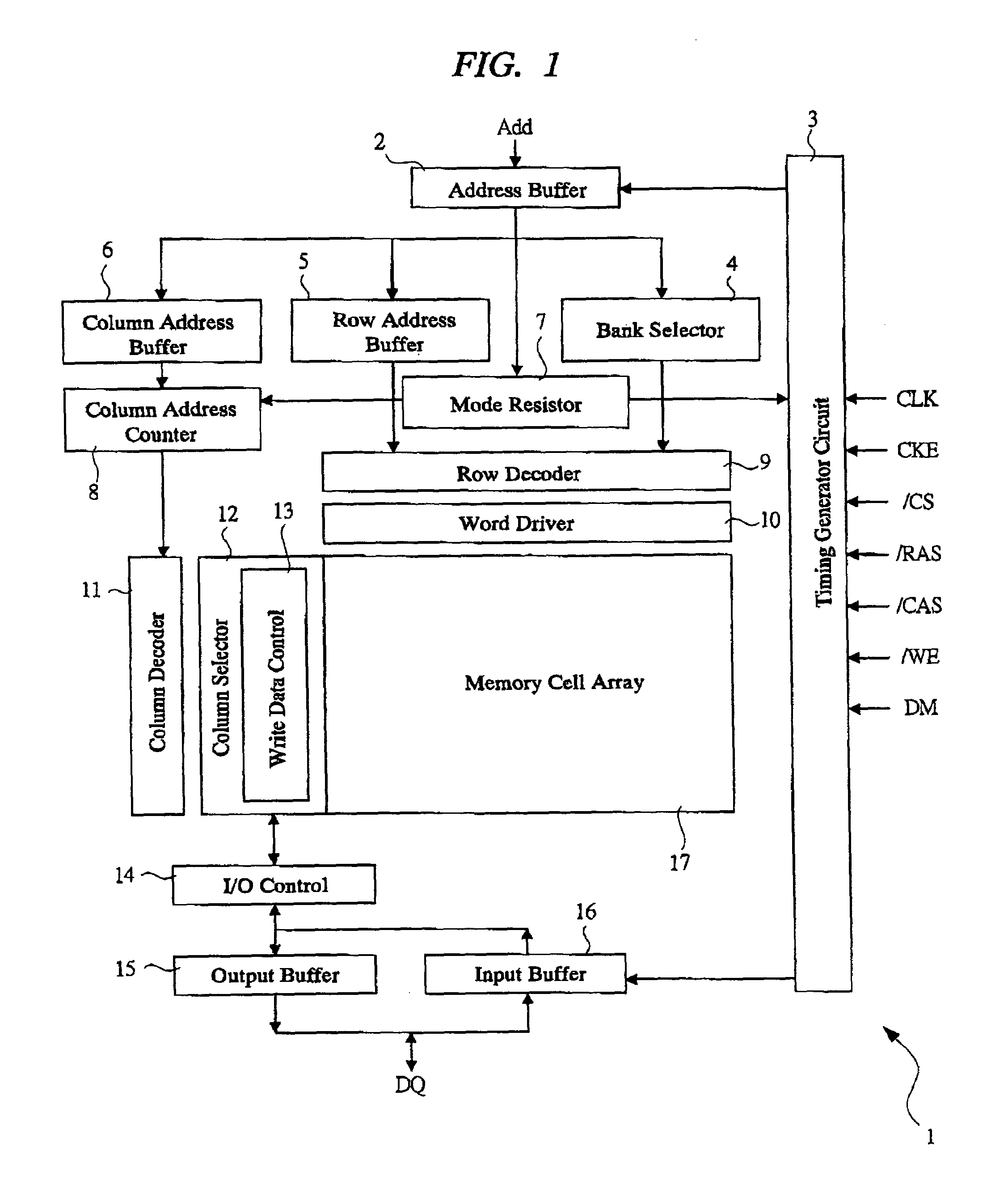
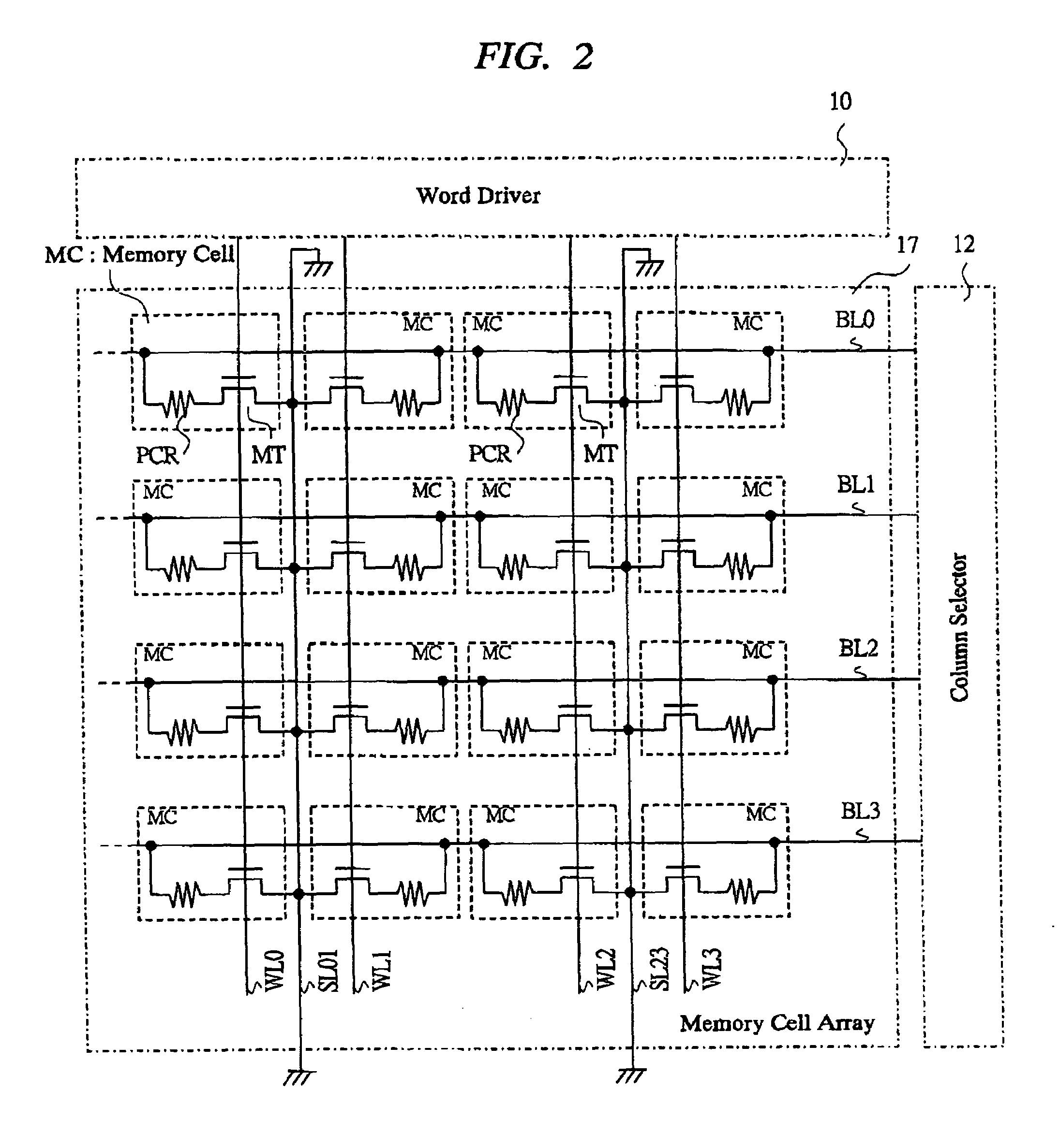
[0050]FIG. 1 is a block diagram of a nonvolatile memory according to a first embodiment of the present invention; FIG. 2 is a circuit diagram showing a configuration example of a memory cell array provided in the nonvolatile memory in FIG. 1; FIG. 3 is a block diagram of a memory cell provided in the memory cell array in FIG. 2; FIG. 4 is a circuit diagram of a column selector provided in the nonvolatile memory in FIG. 1; FIG. 5 is a circuit diagram showing one example of a pre-charge circuit provided in the column selector in FIG. 4; FIG. 6 is a circuit diagram showing one example of a sense amplifier provided in the column selector in FIG. 4; FIG. 7 is a circuit diagram showing one example of a write driver provided in the column selector in FIG. 4; FIG. 8 is a timing chart of a write operation in the nonvolatile memory in FIG. 1; FIG. 9 is a timing chart of a read operation in the nonvolatile memory in FIG. 1; FIG. 10 is a timing chart showing another example of a write operation...

second embodiment

[0151]FIG. 12 is a circuit diagram of a column selector provided in a nonvolatile memory according to a second embodiment of the present invention; FIG. 13 is a circuit diagram of a write driver provided in the column selector of FIG. 12; FIG. 14 is a timing chart showing one example of a write operation by a nonvolatile memory according to a second embodiment of the present invention; and FIG. 15 is a timing chart showing another example of a write operation by a nonvolatile memory according to a second embodiment of the present invention.

[0152]In the second embodiment, the nonvolatile memory has the same configuration as that of the above-described first embodiment, but is different therefrom in a circuit configuration of a column selector 12a.

[0153]FIG. 12 is a circuit diagram showing a portion of the column selector 12a.

[0154]A column selector 12a simultaneously performs processes for changes to low-resistance and high-resistance states per column cycle in the same period.

[015...

third embodiment

[0187]FIG. 16 is a circuit diagram of a column selector provided in a nonvolatile memory according to a third embodiment of the present invention; FIG. 17 is a circuit diagram of a write driver provided in the column selector of FIG. 16; FIG. 18 is a timing chart showing one example of a write operation by a nonvolatile memory according to a third embodiment of the present invention; FIG. 19 is a circuit diagram showing another example of the column selector of FIG. 16; FIG. 20 is a block diagram showing one example of a nonvolatile memory having a refresh operation function, which is a third embodiment of the present invention; FIG. 21 is a circuit diagram showing one example of a memory cell in the nonvolatile memory in FIG. 20; FIG. 22 is a block diagram showing one example of a nonvolatile memory having a data correcting function, which is a third embodiment of the present invention; and FIG. 23 is a circuit diagram showing one example of a memory cell array in the nonvolatile m...


PUM


Abstract

There is achieved a high-integrated and high-speed nonvolatile memory which can stabilize an operation of a phase-change memory for a short operation cycle time. A latch is provided in a write driver. A change to a high-resistance state of a phase-change element is performed per column cycle by a write-enable signal, and a change to a low-resistance state thereof is performed after a pre-charge command is inputted and concurrently with deactivation of a pre-charge signal. Thereby, a write time to a memory cell in which phase-change resistance is changed to a low-resistance state, and a period from a write operation for changing the phase-change resistance to a high-resistance state to a read operation to the above memory cell can be lengthened without extending the column cycle time, so that the stable write operation is achieved.

Description

CROSS-REFERENCE TO RELATED APPLICATION[0001]The present application claims priority from Japanese patent application No. JP 2003-398398 filed on Nov. 28, 2003, the content of which is hereby incorporated by reference into this application.BACKGROUND OF THE INVENTION[0002]The present invention relates to a technique for writing data in a semiconductor integrated circuit device and especially a technique effectively applicable to stabilization of data write in a semiconductor memory, which utilizes a phase-change resistance.[0003]Development of a phase-change memory is advanced in order to achieve a high-speed and high-integrated nonvolatile memory.[0004]In the phase-change memory, a phase-change material called a chalcogenide material stores data by utilizing a resistance property depending on its states.[0005]Rewriting of the phase-change resistance is performed by changing its state by applying a current thereto and generating heat. A change to a low-resistance state, which is call...

Claims


Application Information

Patent Timeline
Patent Type & Authority Patents(United States)
IPC IPC(8): G11C11/34G11C11/42G11C5/00G11C7/00G11C8/08G11C11/419G11C13/02
CPCG11C7/1078G11C7/1087G11C7/1096G11C8/08G11C13/0004G11C13/0028G11C13/004G11C13/0069G11C2213/79G11C13/0033G11C7/1069
Inventor TAKEMURA, RIICHIROSAKATA, TAKESHITAKAURA, NORIKATSUKAJIGAYA, KAZUHIKO
Owner LONGITUDE SEMICON S A R L
Why Eureka
Try Eureka