Placement and routing method to reduce Joule heating

a technology of joule heating and routing method, applied in the field can solve the problems of metal line or dielectric layer stress to the point of failure, metal line to become open circuit, and heat is not efficiently transferred over the metal line, etc., to achieve the effect of reducing joule heating problems

Active Publication Date: 2006-12-26
TAIWAN SEMICON MFG CO LTD
View PDF9 Cites 14 Cited by
  • Summary
  • Abstract
  • Description
  • Claims
  • Application Information

AI Technical Summary

Benefits of technology

[0014]A principal object of the present invention is to provide an effective method to reduce Joule heating problems in an integrated circuit device.
[0020]A yet further object of the present invention is to eliminate Joule heating problems without requiring larger metal line widths.
[0021]Another further object of the present invention is to provide a signal routing structure having improved Joule heating performance.
[0023]In accordance with the objects of this invention, a method to optimize a signal routing in an integrated circuit is achieved. The method comprises providing a signal routing in an integrated circuit layout. The signal routing comprises a configuration of metal lines in a stack of metal levels. Each metal level is separated from an underlying substrate by dielectric material. A Joule heating estimate is calculated for the signal routing. The Joule heating estimate is compared to a standard value. The signal routing is updated if the Joule heating estimate exceeds the standard value. The updating comprises generating a new configuration of the metal lines in the metal levels. The new configuration reduces the Joule heating. The steps of calculating, comparing, and updating are repeated if the Joule heating estimate still exceeds the standard value.

Problems solved by technology

Typically, the heat is not efficiently transferred above the metal lines 18 because the overlying materials are not primarily good thermal conductors.
If the signal line temperature becomes excessive, the metal line or the dielectric layers can be stressed to the point of failure.
Electromigration can cause a metal line to become open circuits.

Method used


Image

  • Placement and routing method to reduce Joule heating
  • Placement and routing method to reduce Joule heating
  • Placement and routing method to reduce Joule heating

Examples


Embodiment Construction

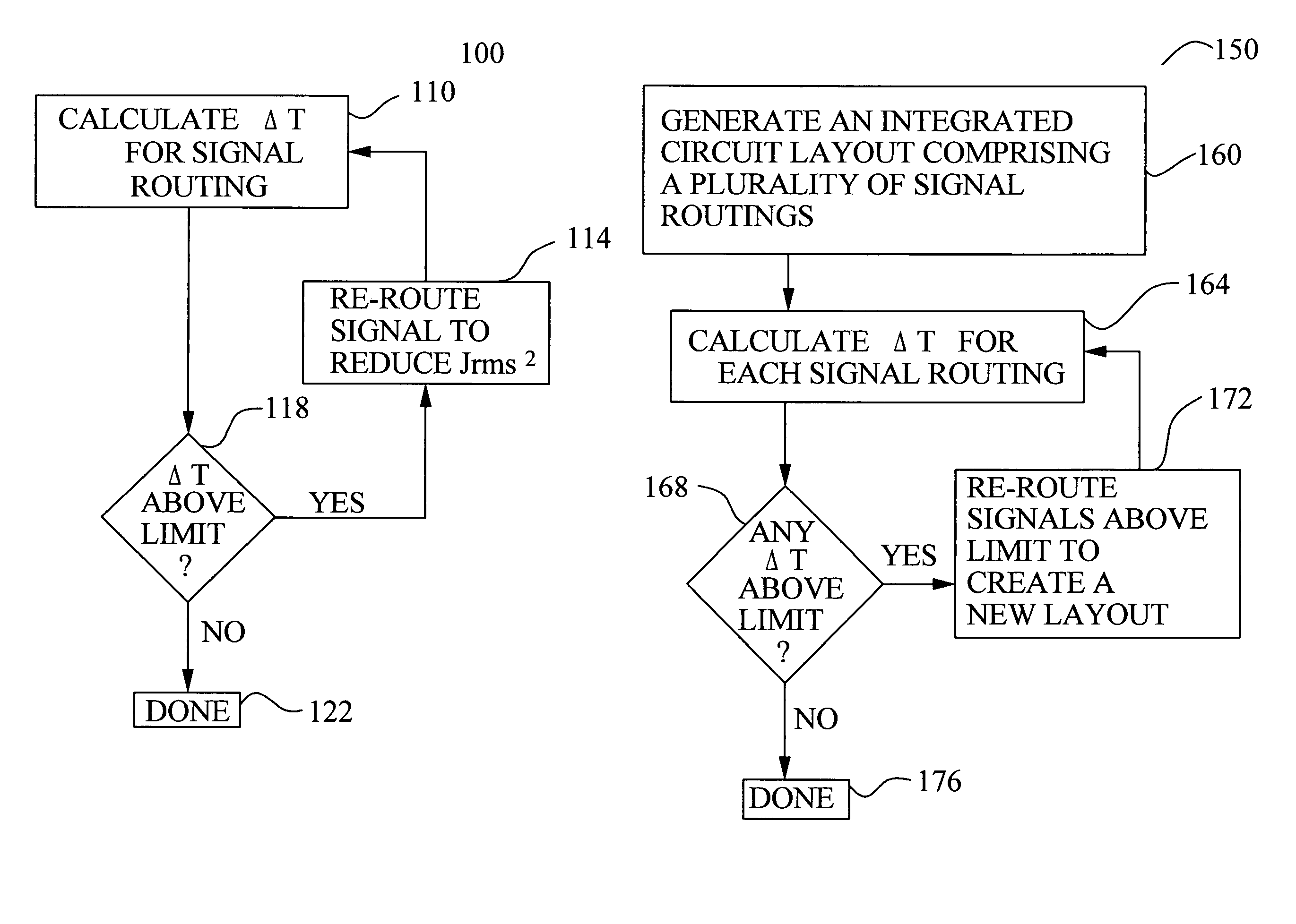
[0037]The preferred embodiments of the present invention disclose a method to prevent Joule heating reliability failures in an integrated circuit device. The method detects signal routings where excessive Joule heating could occur. These signals are re-routed to reduce the Joule heating. The re-routing comprises either moving part of the signal path to a lower metal level or coupling the signal routing to a heat sink. It should be clear to those experienced in the art that the present invention can be applied and extended without deviating from the scope of the present invention.

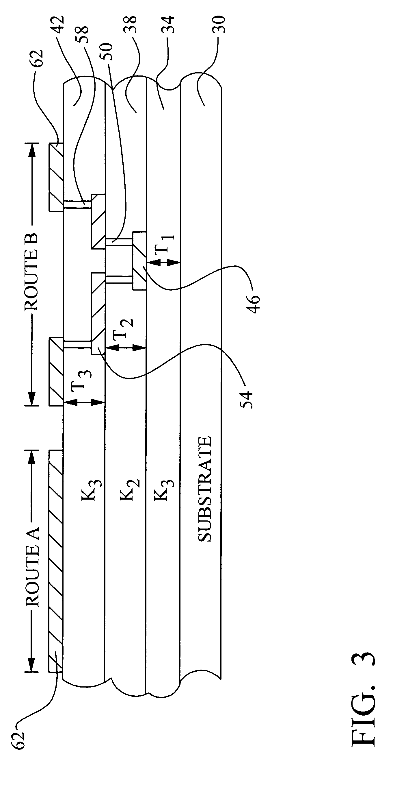
[0038]Referring now to FIG. 3, a simplified cross section of an integrated circuit device is illustrated. The device comprises a substrate 30 as is typical to the art. Three metal layers 46, 54, and 62 are formed overlying the substrate 30. Three dielectric layers 34, 38, and 42 are formed overlying the substrate and serve to separate the three metal layers 46, 54, and 62. Further, vias 50 and 58 are formed ...


PUM


Abstract

A new method to optimize a signal routing in an integrated circuit is achieved. The method comprises providing a signal routing in an integrated circuit layout. The signal routing comprises a configuration of metal lines in a stack of metal levels. Each metal level is separated from an underlying substrate by dielectric material. A Joule heating estimate is calculated for the signal routing. The Joule heating estimate is compared to a standard value. The signal routing is updated if the Joule heating estimate exceeds the standard value. The updating comprises generating a new configuration of the metal lines in the metal levels. The new configuration reduces the Joule heating. The steps of calculating, comparing, and updating are repeated if the Joule heating estimate still exceeds the standard value. Joule heating is reduced by either routing on lower metal levels or by coupling the signal routing to a heat sink.

Description

BACKGROUND OF THE INVENTION[0001](1) Field of the Invention[0002]The invention relates to a method to reduce Joule heating in an integrated circuit device, and, more particularly, to a method to detect Joule heating problems in signal routes and to eliminate these problems through re-routing or through a heat sink.[0003](2) Description of the Prior Art[0004]Integrated circuit devices typically contain a large number of signal wires, or lines. These signal lines are formed in a conductive layer such as a metal film. Individual signal lines are separated using dielectric films. The combination of signal lines and dielectric films creates a set of interconnect levels for an integrated circuit device. It is common for an integrated circuit device to use eight or more levels of interconnect formed in a stack and using via openings to allow connection between adjacent levels.[0005]Referring now to FIG. 1, a simplified cross section of an integrated circuit device is shown. The cross secti...

Claims


Application Information

Patent Timeline
Patent Type & Authority Patents(United States)
IPC IPC(8): G06F17/50H01L21/768H01L23/52H01L23/528H01L23/535
CPCG06F17/5077H01L23/3677G06F2217/80H01L2924/0002H01L2924/00G06F30/394G06F2119/08
Inventor HOU, CHIN-SHANONG, TONG-CHERNYANG, JUI-LINGWU, JUN-YI
Owner TAIWAN SEMICON MFG CO LTD
Why Eureka
Try Eureka