
Scanning electrochemical potential microscope

a potential microscope and scanning electrode technology, applied in the direction of liquid/fluent solid measurement, material electrochemical variables, instruments, etc., can solve the problems of high concentration of solution, compromising image resolution, compromising image integrity, etc., and achieve high resolution

Inactive Publication Date: 2007-01-02
BRUKER NANO INC
View PDF10 Cites 27 Cited by
  • Summary
  • Abstract
  • Description
  • Claims
  • Application Information

AI Technical Summary

Benefits of technology

The preferred embodiment of this patent is a scanning electrochemical potential microscope (SEPM) that uses a passive probe to characterize a sample surface at high resolution. The SEPM is capable of operating at rest and at reactive potentials, and can image poorly conductive samples on either conducting or semi-conducting surfaces. It can measure the potential across an electrical double layer at a surface of a sample, and can generate a topography map of the surface by moving the tip of the probe in response to a feedback signal. The SEPM can also compare the measured potential with a standard potential to determine a charge distribution associated with the sample. The invention provides a better understanding of the potential distribution on a sample surface, and can be used in various fields such as materials science and biological research.

Problems solved by technology

In addition, even for STM applications in solution, the tunneling current is non-faradaic (i.e., no chemical changes in solution components or sample surface species occur due to the tunneling current), so that unlike SECM, the tip current cannot be related directly to the sample potential.
In addition to the above, both STM and SECM have other significant drawbacks for electrochemical applications.
In electrochemical STM, the highly concentrated solution compromises image resolution by interfering with the tunneling current.
Moreover, for biological applications, because the tip-substrate separation is extremely small (less than 1 nanometer, as mentioned above), if the biological object is relatively large, the tip may penetrate into the object being scanned, thus clearly compromising the integrity of the image.
This is exacerbated by the fact that biological molecules are poor conductors, thus providing no relief with respect to the narrow tip-sample separations.
For example, if one places a DNA molecule on top of a conducting substrate and tries to perform STM to characterize the DNA molecule, it will be extremely difficult to generate sufficient current to pass through the molecule.
Thus, some sample measurements are impossible with an STM.
Further, even if the sample is an adequate conductor, the STM is limited by the fact that, because it does not operate based on force feedback, the user is often unaware of how much force the STM tip is exerting on the sample, thus leading to damaged samples.
Larger tip-sample working distances yield very poor resolution and thus, in essence, the preferred SECM working distance is too great.
Although this aspect of the system affords SECM the ability to perform a wide range of applications such as etching, etc., a major drawback in this regard is that it is difficult to maintain reliable operability of the electrodes for extended periods of time.
However, the spatial resolution is only about a few tens of micrometers, again unacceptable for the presently contemplated applications.
This indirect measurement of DNA hybridization, although time efficient once the sample is prepared, is an expensive and very labor intensive process primarily due to the aforementioned sample preparation.
Moreover, requiring an optical microscope has significant disadvantages, such as non-ideal resolution.
As a result, unfortunately, single molecules of DNA cannot readily be measured and imaged with the gene chip.
In addition to this drawback, using the PCR technique is impossible for some types of samples.
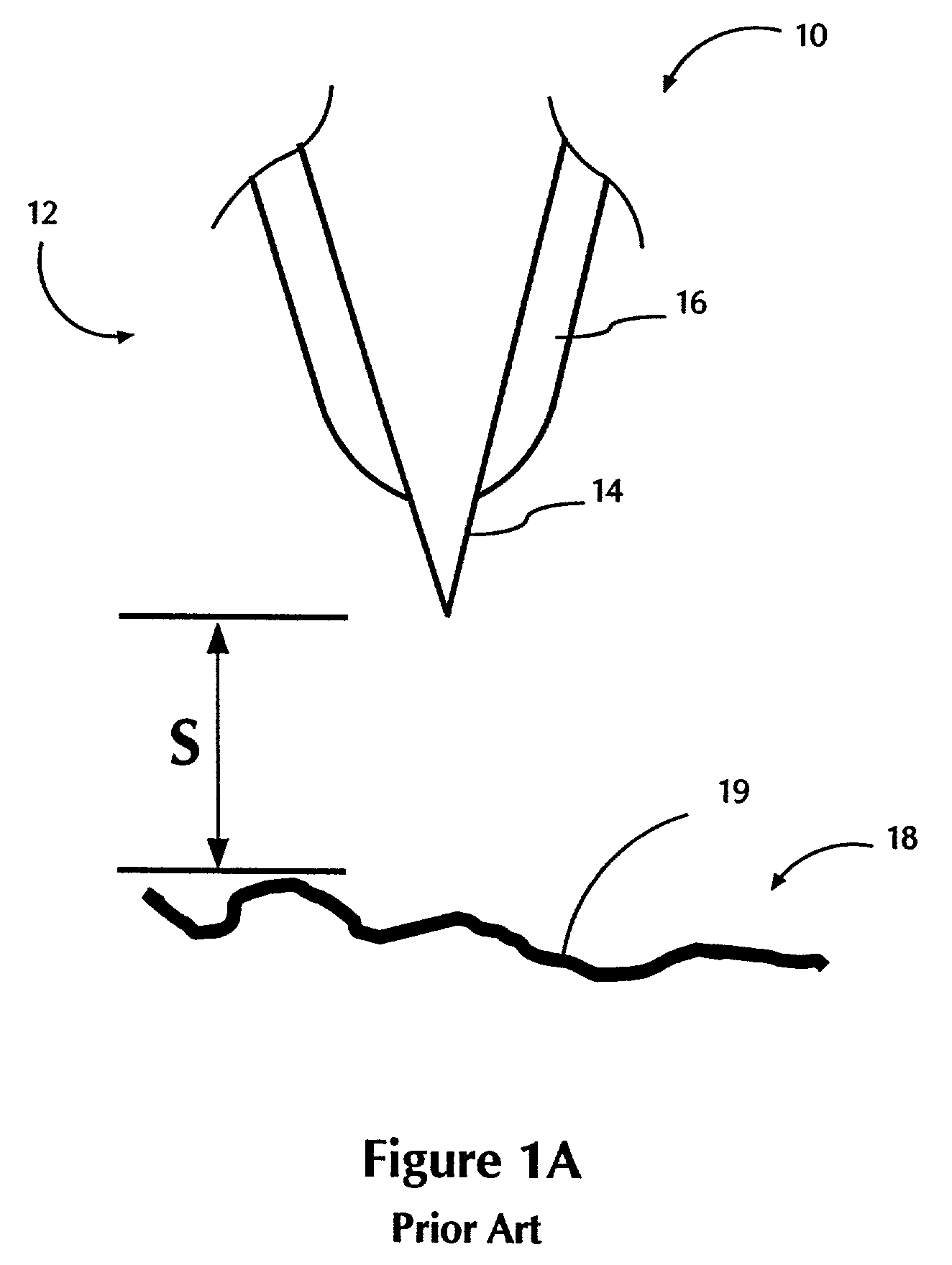
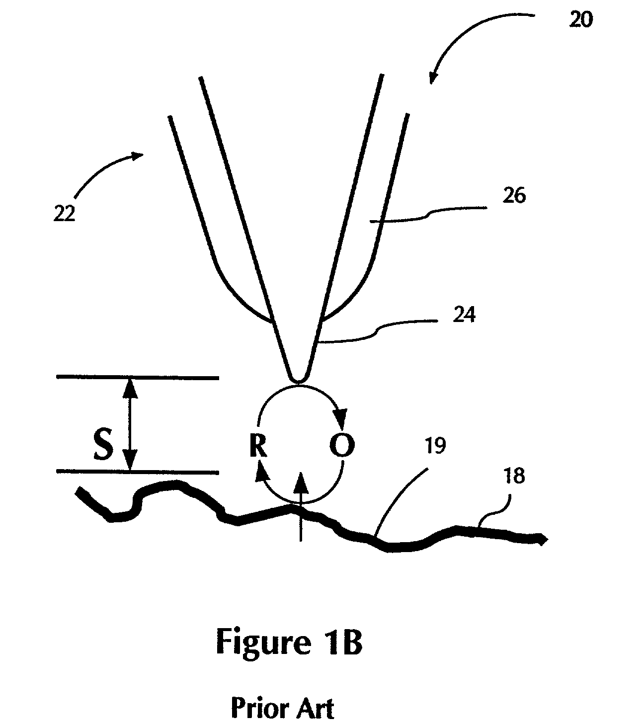
In sum, in both SECM and STM, a significant drawback is that each system requires current flow between the tip and sample, as SECM uses electrochemical current and STM uses tunneling current as their respective feedback signal.

Method used


Image

  • Scanning electrochemical potential microscope
  • Scanning electrochemical potential microscope
  • Scanning electrochemical potential microscope

Examples


Embodiment Construction

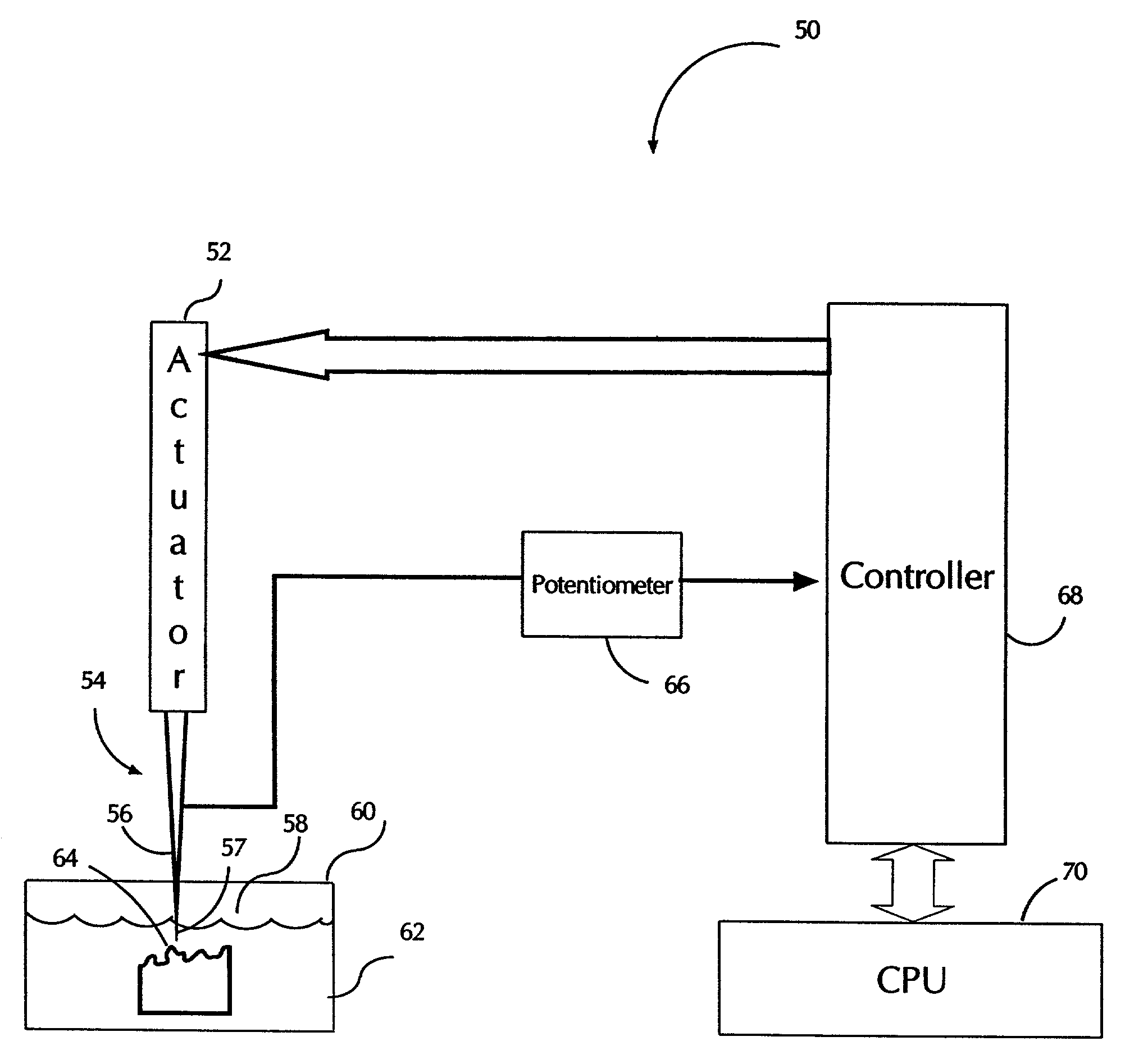
[0058]Turning initially to FIG. 2, a scanning electrochemical potential microscope 50 (SEPM) according to the present invention is used to measure sample characteristics by monitoring an electrical double layer at the sample surface. An illustration of the double layer, including a cross-section of a tip 56 of a probe 54 and a substrate 58 in a scanning electrochemical potential microscope environment is shown in FIG. 3. A key property of the electrical double layer is that, as mentioned previously, the positive and negative ions or molecular dipoles of the layer are ordered in a way that follows the surface in a highly localized way. More generally, SEPM 50 monitors local changes (down to the atomic level) in the double layer that are indicative of sample characteristics.

[0059]To create the electrical double layer, in FIG. 3 for a blown up view, the substrate 58 is disposed in a polar solution such that the double layer is formed adjacent thereto. Separation “S” denotes the perpend...


PUM

PropertyMeasurementUnit
atomic distanceaaaaaaaaaa
working distanceaaaaaaaaaa
charge distributionaaaaaaaaaa

Abstract

An apparatus and method of determining a potential at a surface of a sample in a polar liquid, for example, across an electrical double layer, includes the step of immersing the sample in a polar solution to form a potential gradient at the surface. A tip of a scanning probe microscope probe is then positioned in the solution generally adjacent the surface. During operation, the method includes measuring a potential of the probe. Relative scanning movement between the sample and the probe may be provided, and, in one mode of operation, a feedback signal is generated based on the measured potential. In that case, the tip may be moved generally orthogonal to the surface in response to the feedback signal to maintain a generally constant separation therebetween. The polar solution may have an associated ionic concentration, and the ionic concentration can be modified to tune the operation of the SEPM.

Description

BACKGROUND OF THE INVENTION[0001]1. Field of the Invention[0002]The present invention is directed to scanning probe microscopes, and more particularly, a scanning electrochemical potential microscope (SEPM) for characterizing a sample placed in a liquid by measuring an electrochemical potential that varies across an electrical double layer at the liquid / solid interface.[0003]2. Description of Related Art[0004]Scanning probe microscopes (SPMs), such as the atomic force microscope (AFM), are devices which typically use a sharp tip and low forces to characterize the surface of a sample down to atomic dimensions. Generally, SPMs include a probe having a tip that is introduced to a surface of a sample to detect changes in the characteristics of a sample. By providing relative scanning movement between the tip and the sample, surface characteristic data can be acquired over a particular region of the sample and a corresponding map of the sample can be generated.[0005]In an AFM, for exampl...

Claims


Application Information

Patent Timeline
Patent Type & Authority Patents(United States)
IPC IPC(8): G01N27/416
CPCG01Q60/60B82Y35/00
Inventor LI, CHUNZENGKJOLLER, KEVIN J.
Owner BRUKER NANO INC
Learn More