Information processing apparatus using index and TAG addresses for cache

Inactive Publication Date: 2007-01-02
RENESAS ELECTRONICS CORP
View PDF15 Cites 10 Cited by
  • Summary
  • Abstract
  • Description
  • Claims
  • Application Information

AI Technical Summary

Benefits of technology

[0011]An object of the present invention, therefore, is to avoid bank conflicts, where a DRAM is to be used as the main memory of an information processing apparatus having a cache, by utilizing both accessing according to the corollary of local

Problems solved by technology

Thus once access to a different word line on the same bank is necessitated by writing back (bank conflict), high speed accessin

Method used


Image

  • Information processing apparatus using index and TAG addresses for cache
  • Information processing apparatus using index and TAG addresses for cache
  • Information processing apparatus using index and TAG addresses for cache

Examples


embodiment 1

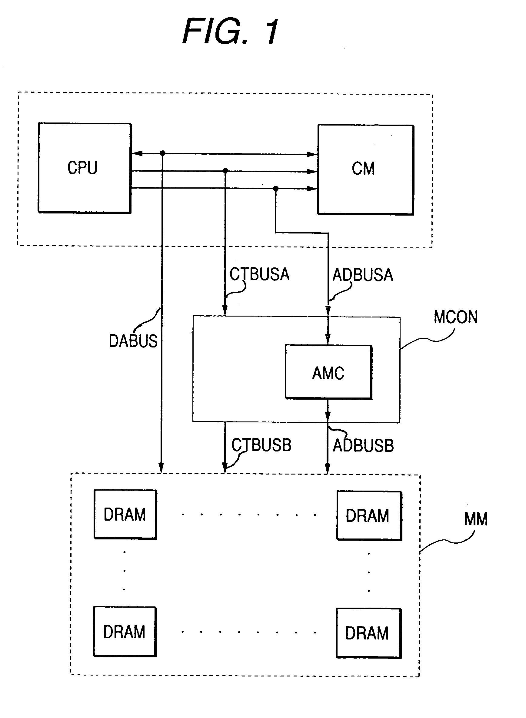
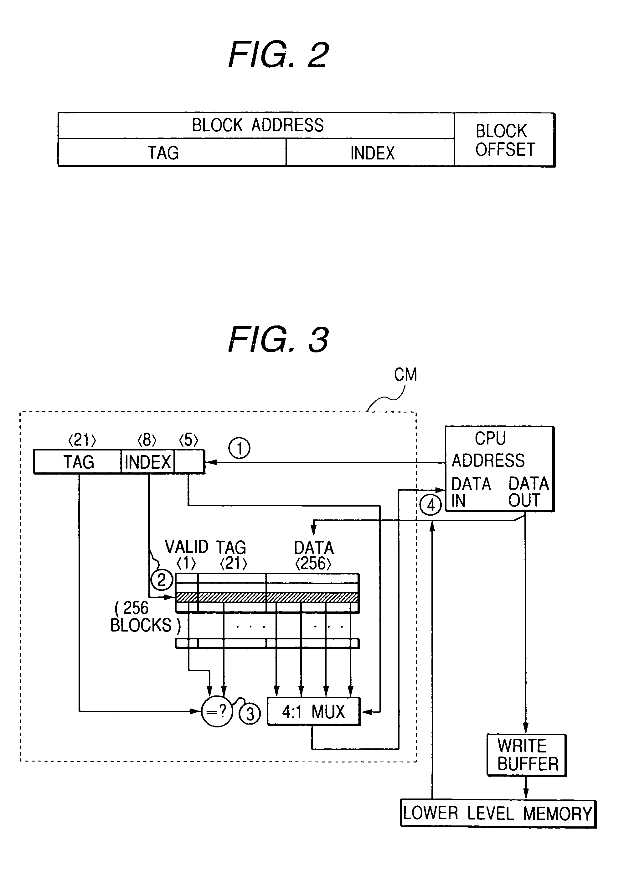
[0027]FIG. 1 is a configurational diagram illustrating the basic concept of the information processing apparatus pertaining to this patent application. This apparatus consists of a cache CM, a CPU, a memory controller MCON involving an address mapping circuit AMC, and a main memory MM comprising one or more DRAMs. A request address from the CPU is communicated to ADBUSA, the CM and the MCON. The request communicated to the CM, after being converted by the AMC into a bank address, a row address and a column address for accessing the DRAM, communicated via ADBUSB to the MM. The description here will refer to a small-scale system for the convenience of explaining address conversion. Accordingly, in the following description, a direct-mapped cache of 128B (in the following description “B” immediately following a numeral denotes “bytes”) in capacity having a block offset of 4 bits (16B). In this example the index consists of 3 bits, and the tag, 23 bits.

[0028]FIG. 4 illustrates an exampl...

embodiment 2

[0033]As stated above, addresses sharing the same index but differing in tag can be assigned to different banks of a DRAM at a high probability without allowing for a bank conflict to arise. As reading and writing at the time of writing back can be assigned to entirely separate banks by extending this address assignment, it is made possible to perform read accessing and write accessing at the time of writing back in the same cycle. An embodiment of this principle will be described below.

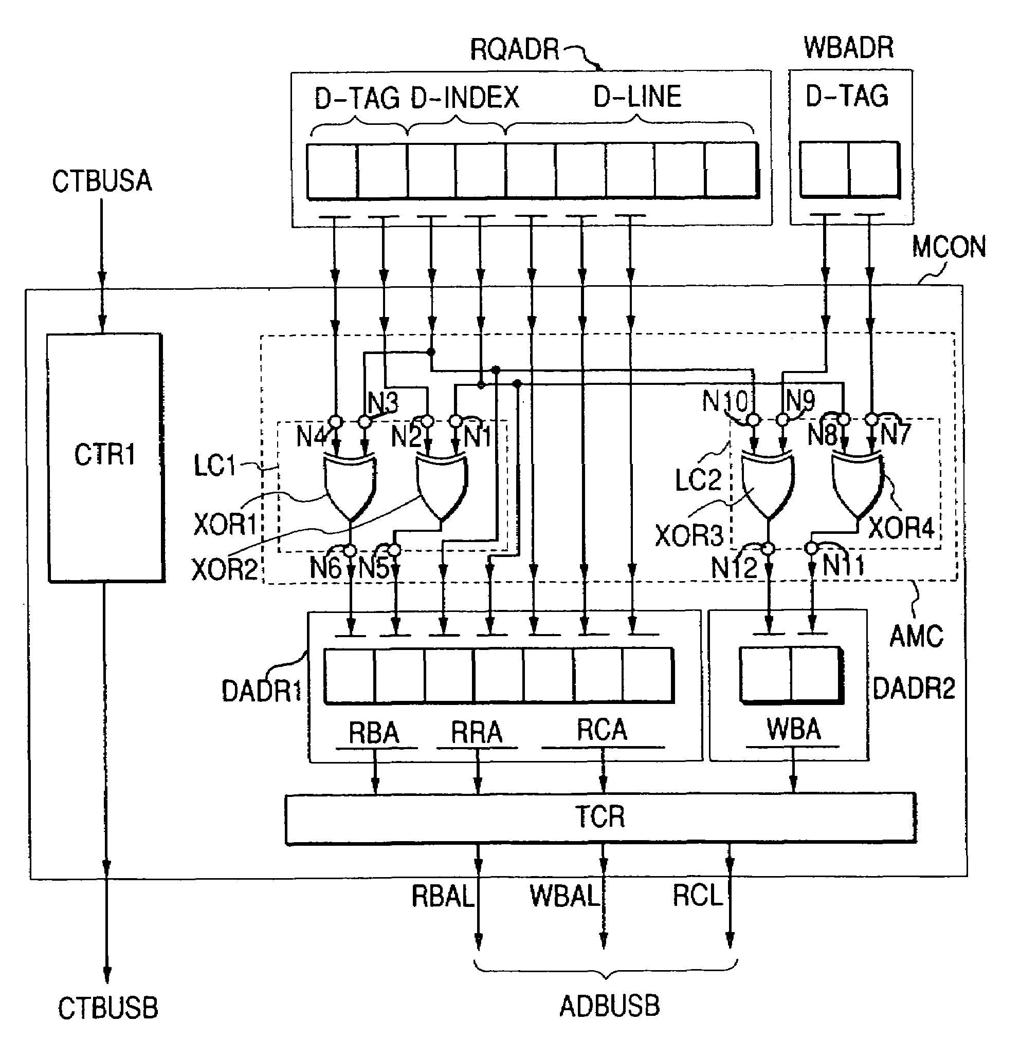
[0034]FIG. 7 illustrates another preferred embodiment of the invention according to which, read accessing and write accessing at the time of writing back (accesses giving rise to replacement of cached contents when a cache is missed) are assigned to completely separate banks and thereby reading and writing at the time of writing back are accomplished at the same time. This embodiment consists of a CPU, a cache CM, a main memory MM involving a DRAM, a memory controller MCON for controlling the MM, and...

embodiment 3

[0052]FIG. 13 illustrates another example of application of the present invention to the information processing apparatus of FIG. 7 in a case where a cache having a typical capacity in current use and a DRAM are disposed. Here is supposed a direct-mapped type write-back system wherein the cache has a capacity of 512 KB and a block offset (LINE) of 32B. In this case, LINE consists of 5 bits (0–4), INDEX, 14 bits (5–18), and the remainder, TAG (19–31). On the other hand, the total capacity of the main memory is supposed to be 128 MB, composed of a DRAM having a multi-bank configuration whose capacity is 8 MB. First, supposing that this 128 MB consists of a single chip DRAM, the earlier defined concept of D-TAG can be applied, so that D-TAG consists of 8 bits. This determines the number of independent banks required by this system to be 256. However, as the capacity of a single chip DRAM is 8 MB, far smaller than such a large required capacity, 16 chips are used to compose the main mem...


PUM


Abstract

In an information processing apparatus involving a cache accessed by INDEX and TAG addresses, accesses to the main memory include many accesses attributable to the local character of referencing and write-back accesses attributable to the replacement of cache contents. Accordingly, high speed accessing requires efficient assignment of the two kinds of accesses to banks of the DRAM. In assigning request addresses from the CPU to different banks of the DRAM, bank addresses of the DRAM and generated by operation of the INDEX field and the TAG field so that local accesses whose INDEX varies and accesses at the time of writing back of which INDEX remains the same but TAG differs can be assigned to different banks. High speed accessing is made possible because accesses to the main memory can be assigned to separate banks. Furthermore, as reading and writing at the time of writing back can be assigned to a separate bank, pseudo dual-port accessing is made possible with only one port, resulting in higher speed write-back accessing.

Description

[0001]This is a continuation application of U.S. Ser. No. 10 / 186,891, filed Jul. 2, 2002 now U.S. Pat. No. 6,715,025, which is a continuation application of U.S. Ser. No. 09 / 495,954, filed Feb. 2, 2000 (now U.S. Pat. No. 6,438,641).FIELD OF THE INVENTION[0002]The present invention relates to an information processing system including a CPU and memories, and more particularly addressing the main memory where a cache is used.BACKGROUND OF THE INVENTION[0003]References cited herein are listed below, and they will be referred to hereinafter by the respective reference numbers. Reference 1 (Ref. 1) corresponds to the following article: Nikkei Microdevices, February 1998, pp. 134–141 (in Japanese), and Reference 2 (Ref. 2) corresponds to the following article: David A. Patterson and John L. Hennessy, Computer Architecture, A Quantitative Approach; Second Edition, Morgan Kaufmann Publisher Inc., (1996), pp. 375–384.[0004]Reference 1 discloses an example of address mapping in a DRAM on p. 1...

Claims


Application Information

Patent Timeline
IPC IPC(8): G06F12/12G06F13/00G06F12/06G06F12/08
CPCG06F12/0882G06F12/0607
Inventor KANNO, YUSUKEMIZUNO, HIROYUKIWATANABE, TAKAO
Owner RENESAS ELECTRONICS CORP
Why Eureka
Try Eureka