
Apparatus and method for testing a device for storing data

a technology for storing data and apparatus, applied in the direction of measurement devices, error detection/correction, instruments, etc., can solve problems such as chip failure, and achieve the effect of less costly testing

Inactive Publication Date: 2007-01-02
POLARIS INNOVATIONS LTD
View PDF10 Cites 1 Cited by
  • Summary
  • Abstract
  • Description
  • Claims
  • Application Information

AI Technical Summary

Benefits of technology

[0010]The object of the present invention is therefore to provide an apparatus and a method for testing a device for storing data and a circuit board which permit less costly testing of a device for storing data.
[0014]An advantage of this preferred development is that, for example, there is, on a circuit board of every base of a storage device, for example a memory chip, a comparison device, for example a logic gate, which logically links the individual results so that it is sufficient if only a single comparator line is led to each of these gates. This not only enables the layout or the design of the circuit board, for example of the burn-in board, to be simplified but additionally considerably reduces the number of comparator channels which are required on a test apparatus, which under certain circumstances permits more components to be mounted on the circuit board.
[0015]Earlier, comparator lines were led to each of the pins of a memory chip. The invention makes it possible to lead only a single line to the gate which is located directly on the base and whose result is then evaluated. If the number of lines is thus greatly reduced in the design, these lines cannot only be laid more easily, because it is necessary to allow for a much smaller number of intersection points, but also the lines can be made wider, which results in lower costs.
[0020]One advantage of these preferred developments is that the use of a single logic element in the vicinity of the base of a storage device simplifies the complexity of the design of, for example, a circuit board.

Problems solved by technology

If it is assumed, for example, that a logic “1” is to be stored in each cell of the memory chip but a logic “0” occurs at least once in a memory cell during the reading out of the actually stored data, then the chip is faulty.
However, in order to save chip area, different degrees of data compression are generally not implemented so that the test result is output at a plurality of pins, which does not constitute an optimum state for the burn-in-board level.
A disadvantage of implementing memory chips so that the test results are output at a plurality of pins of the memory chip is that, for example, a line of a comparator has to be led to each of the pins which supply test results during the test of the memory chip on the burn-in board, and the signals on the individual lines in a test device have to be compared, for example using an OR logic element if a logic “1” corresponds to a defect, in order to be able to determine the status of the memory chip.

Method used


Image

  • Apparatus and method for testing a device for storing data
  • Apparatus and method for testing a device for storing data

Examples


Embodiment Construction

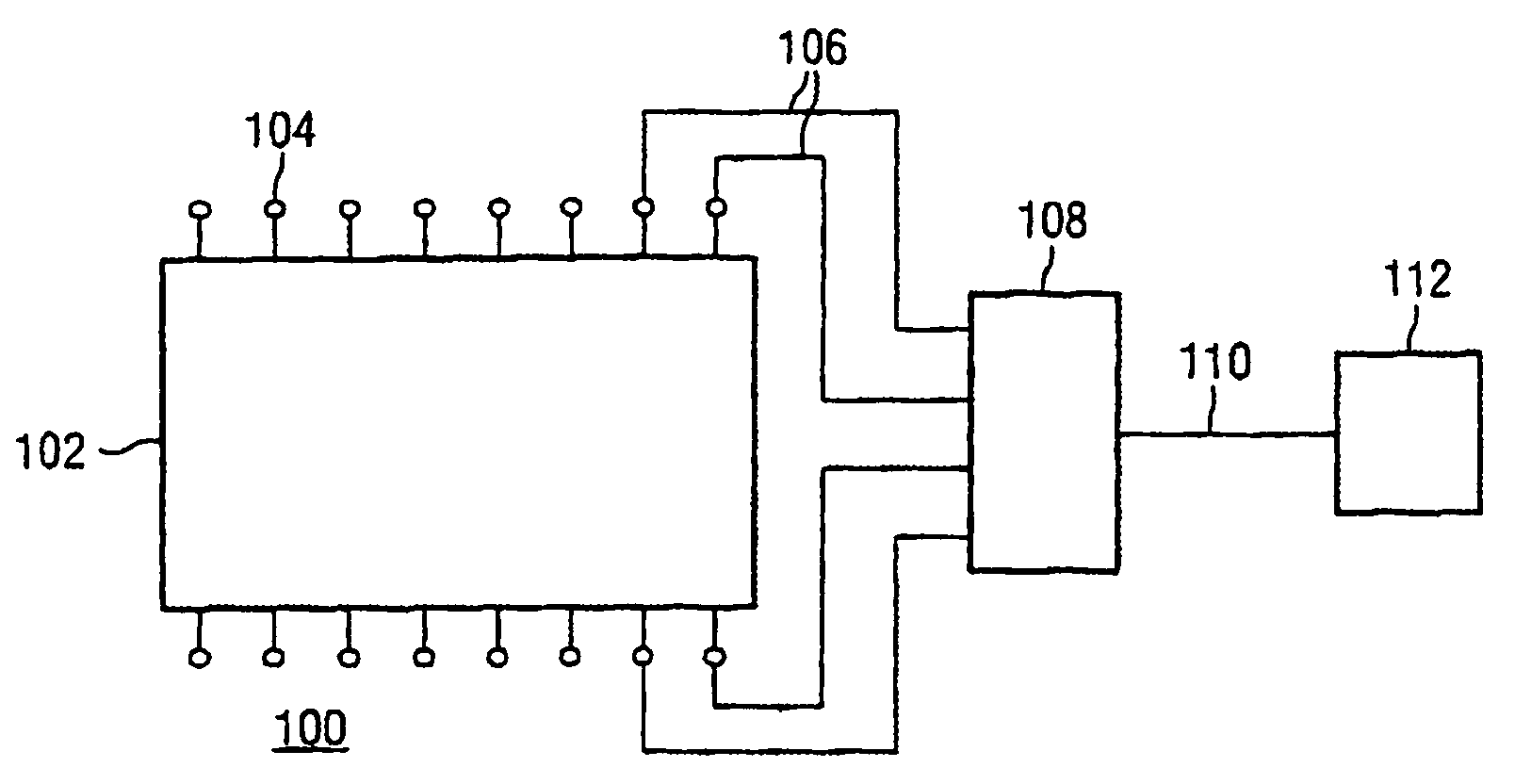
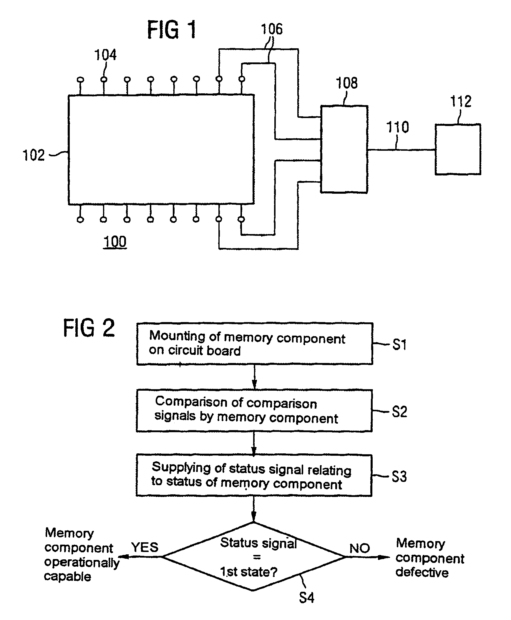
[0030]The storage device 102 has a plurality of storage areas which are, for example, each composed of a plurality of memory cells and a plurality of pins 104, for example contact pins for inputting and outputting data. In addition, the storage device 102 has a device for comparing actual data with set point data for individual storage areas of the plurality of storage areas, and a device for supplying a comparison signal 106 for each storage area. The comparison signal 106 has a first state if the actual data is identical to the set point data, and has a second state if the actual data is not identical to the set point data. Each comparison signal which is assigned to a storage area is respectively output at a pin of the plurality of pins 104 of the device for storing data.

[0031]If a “1” is to be stored, for example, in a memory cell of a storage area of a storage device, for example a memory chip, but “0” occurs during the reading out of the actually stored data, the memory cell, ...


PUM


Abstract

The present invention provides an apparatus for testing a device (102) for storing data, which has a device for comparing actual data with set point data for individual storage areas and a device for supplying a comparison signal (106) for each storage area, which comparison signal (106) has a first state if the actual data is identical to the set point data, and a second state if the actual data is not identical to the set point data. The testing apparatus has a circuit board (100) on which the storage device (102) can be mounted, and a device (108) for comparing the states of the comparison signals at the pins of the storage device (102) which are assigned to the comparison signals (106), and for supplying a status signal (110) which, as a function of the state of the comparison signal, has a first state if the storage device (102) is operationally capable, and has a second state if the storage device (102) is defective.

Description

TECHNICAL FIELD[0001]The present invention relates to an apparatus and a method for testing a device for storing data and to a circuit board.BACKGROUND ART[0002]Memory chips are tested, inter alia, at the front end, i.e. at the wafer level, if the wafer has not yet been sawn into individual components and they are not yet located in housings or tested on burn-in boards. Front-end testing has the advantage that contact can be made with specific points on the chip using sharp needles and voltages or currents can be measured. Once the chip is mounted in its housing, these measuring points can no longer be accessed from the outside. Burning-in is an artificial aging of chips at a high temperature and high operating voltage. If the error rate of memory chips is plotted against their age, a characteristic curve is obtained which is similar to the shape of a bathtub, i.e. most chips are defective from the start or only have a defect after a relatively long time. For this reason, these chip...

Claims


Application Information

Patent Timeline
Patent Type & Authority Patents(United States)
IPC IPC(8): G11C29/00G11C29/48G11C29/56
CPCG11C29/56G11C29/48
Inventor FINTEIS, THOMAS
Owner POLARIS INNOVATIONS LTD
Learn More