IBIST interconnect and bridge fault detection scheme

Active Publication Date: 2007-01-09
ORACLE INT CORP
View PDF5 Cites 8 Cited by
  • Summary
  • Abstract
  • Description
  • Claims
  • Application Information

AI Technical Summary

Problems solved by technology

As fabrication and miniaturization techniques advance, the possibility of certain defects in the fabricated part may increase.
These bridge defects results in an inability to simultaneously send and/or receive distinct signals fr

Method used


Image

  • IBIST interconnect and bridge fault detection scheme
  • IBIST interconnect and bridge fault detection scheme
  • IBIST interconnect and bridge fault detection scheme

Examples


Embodiment Construction

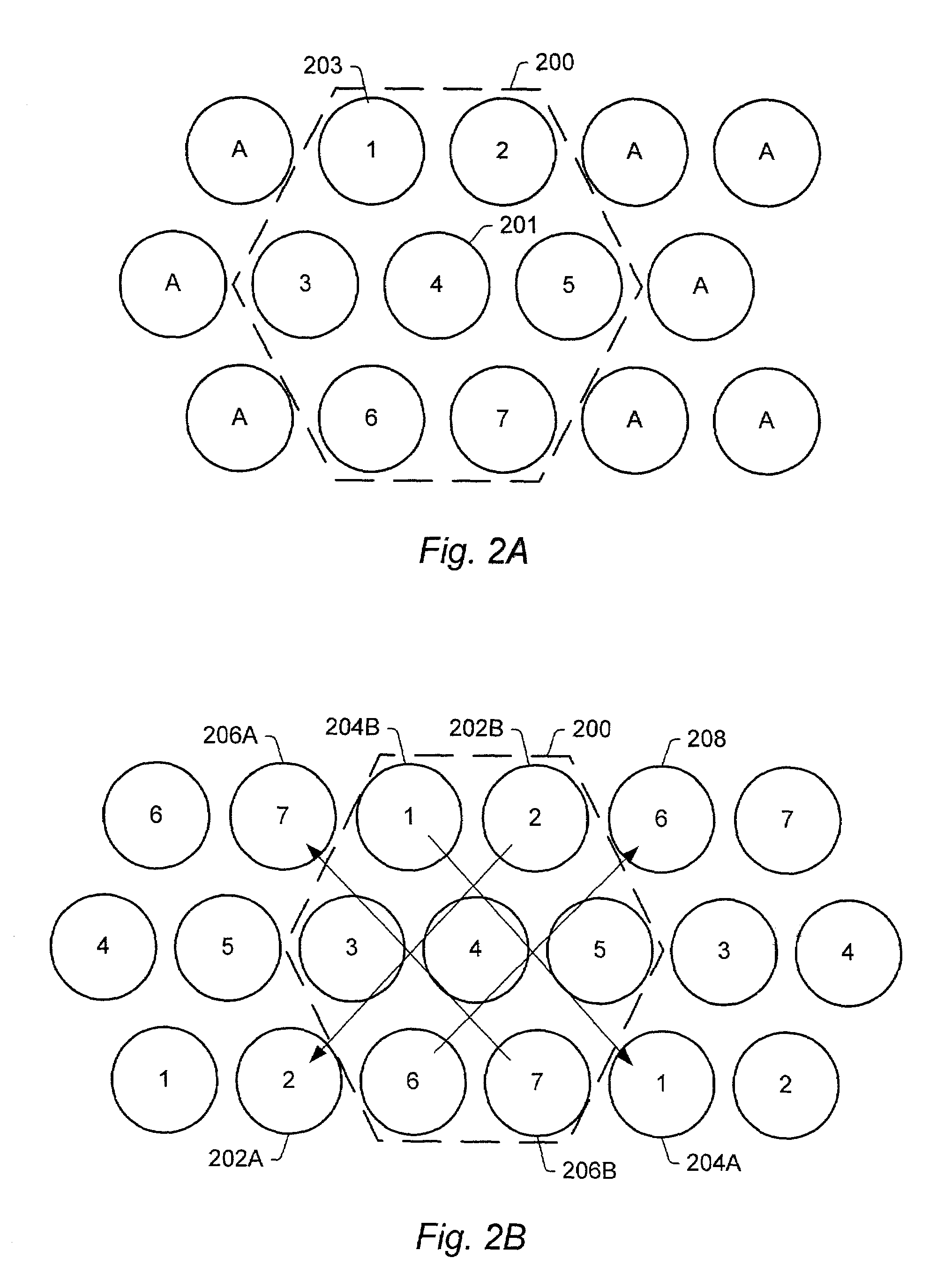
[0018]In the following discussion, a BGA type packaging will be used for illustrative purposes. However, it is understood that the method and mechanism described herein may be applied to devices manufactured according to different techniques. In addition, an array of seven contact points and placement designations will be used for purposes of discussion. However, other configurations, designations schemes with fewer or more designations, and other arrangements are contemplated as well.

[0019]FIG. 2 illustrates an array of contact points denoted “1”–“7” and “A” which may comprise a portion of a chip or circuit to be tested. In the example shown, a group of contact points 200 have been demarcated by a hexagon for purposes of discussion. Included in group 200 are seven contact points which have been arbitrarily numbered from 1 to 7. From the illustration, it can be seen that the contact point numbered 4 is adjacent to six other contact points, 1–3 and 5–7. Consequently, the possible bri...


PUM


Abstract

A method and mechanism for detecting interconnect and bridge defects. Contact points in a chip are assigned placement designation such that no two adjacent points have the same designation. A transmitter, receiver, and optional transmitter/receiver test are then run. During the transmitter test, transmitters with a given designation drive a particular test pattern while other transmitters drive a different test pattern. Receivers compare received test patterns against expected patterns. During a receiver test, transmitters drive a test pattern corresponding to the placement designation of the receivers to which they are coupled. During a particular receiver test, transmitters coupled to receivers of a given designation drive a particular stream, while other transmitters drive a different stream. Receivers then compare received streams against an expected stream. Finally, the placement designation of a transmitter or receiver of an adjacent transmitter/receiver pair may be temporarily assigned an alternate designation. A transmitter or receiver test is then run and receivers check received test patterns against expected patterns.

Description

BACKGROUND OF THE INVENTION[0001]1. Field of the Invention[0002]This invention is related to the field of digital communications and, more particularly, to the test and debug of digital systems.[0003]2. Description of the Related Art[0004]As dependence on various electronic systems continues to increase, so too does the need for reliability. From a hardware perspective, reliability may be ascertained by testing at various levels. These levels of testing include system tests, printed circuit assembly (i.e. circuit board) tests and integrated circuit tests. Such tests seek to ensure proper fabrication and assembly of the various components of the system.[0005]Numerous well known methods of test and debug exist for the purpose of debugging circuits and systems. One such method is to incorporate “built-in self test” (BIST) functionality into the design of a computer system. BIST involves moving test functionality directly onto the chip itself. With BIST functionality designed into a sys...

Claims


Application Information

Patent Timeline
IPC IPC(8): G01R31/28G01F11/00G01R31/26H04L12/46
CPCH04L12/4625
Inventor SMITH, BRIAN L.
Owner ORACLE INT CORP
Why Eureka
Try Eureka