DRAM test method and device, readable storage medium and electronic equipment

A test method and technology to be tested, applied in static memory, instruments, etc., can solve problems such as faulty cell storage errors, and achieve the effects of improving product health, improving fault coverage, and enhancing reliability

Pending Publication Date: 2021-04-02
BIWIN STORAGE TECH CO LTD
View PDF0 Cites 0 Cited by
  • Summary
  • Abstract
  • Description
  • Claims
  • Application Information

AI Technical Summary

Problems solved by technology

[0007] Coupling faults are easier to be excited under special circumstances. One of the situations is that a certain cell is at high level, but the surrounding cells are all at low level, or on the contrary, a certain cell is at low level, but its other cells are at low level. The surrounding cells are all high level, and this large-span potential difference easily triggers storage errors in faulty cells
There is currently no means of testing for this failure condition

Method used


Image

  • DRAM test method and device, readable storage medium and electronic equipment
  • DRAM test method and device, readable storage medium and electronic equipment
  • DRAM test method and device, readable storage medium and electronic equipment

Examples


Embodiment 1

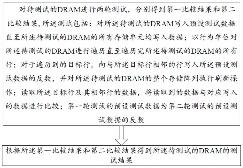
[0088] Please refer to figure 1 , a kind of DRAM test method, comprises steps:

[0089] S1. Carrying out two rounds of tests on the DRAM to be tested, and obtaining a first comparison result and a second comparison result respectively;

[0090] The tests include:

[0091] S11. Writing preset test data to the DRAM to be tested until all storage units of the DRAM to be tested are written with data;

[0092] Specifically, the preset test data is written from the low-order address of each first preset read-write unit of the DRAM to be tested in units of a preset burst length until all storages of the DRAM to be tested are All units are written with data;

[0093] Wherein, the first preset read-write unit can be flexibly set according to actual needs, for example, it can be set as columns or rows;

[0094] The burst length (Burst Length, BL) is determined by the JEDEC standard, and can also be set freely, that is, multiple bits (such as 8 bits or 16 bits) are operated at a time...

Embodiment 2

[0135] The difference between the second embodiment and the first embodiment is that the first preset unit is a column, and the preset sequence is to perform read and write operations on the next row of the target row first, and then perform read and write operations on the previous row of the target row. read and write operations;

[0136] Specifically, the address to be located is column 0, row 0, and the test data D is written from the memory cell corresponding to column 0, row 0 by pressing BL, that is, writing from column 0, row 0 to column 7, row 0 After writing the test data D, start writing the test data D from column 0 and row 1. After writing all the rows from column 0 to column 7, write all the rows from column 8 to column 15 in the order of rows. row, and so on, until the entire storage array has written data;

[0137] Secondly, in row units, start traversing the storage array from row 0 until traversing all the rows of the entire storage array. For the traversed ...

Embodiment 3

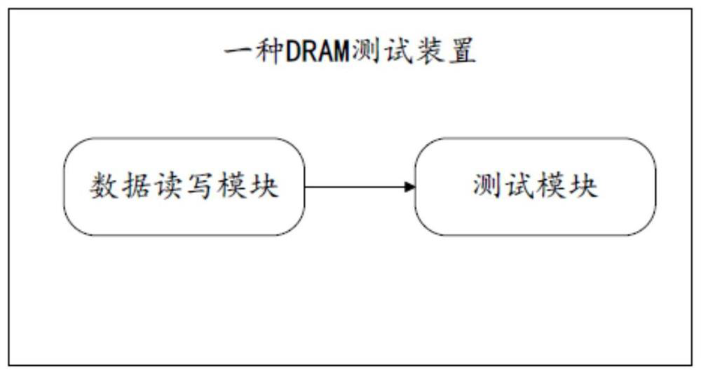
[0151] Please refer to figure 2 , a DRAM testing device, comprising:

[0152] The data reading and writing module is used to carry out two rounds of tests on the DRAM to be tested, and obtain the first comparison result and the second comparison result respectively;

[0153] The tests include:

[0154] Writing preset test data to the DRAM to be tested until all memory cells of the DRAM to be tested are written with data;

[0155] Traversing the DRAM to be tested in row units until all rows of the DRAM to be tested are traversed;

[0156] For the traversed target row, write the inverse of the preset test data to a row adjacent to the target row, and perform a refresh operation on the entire storage array of the DRAM to be tested;

[0157] Read the data of the target row and its adjacent rows, and compare the read data with the corresponding written data;

[0158] The preset test data of the first round of testing is the inverse of the preset test data of the second round o...


PUM


Abstract

According to the invention, the DRAM to be tested is subjected to two rounds of testing, all the storage units written with the preset testing data are subjected to row alternate access, the comparison result is obtained in the row alternate access process, and the final testing result is obtained through the comparison result of the two rounds of testing; the invention can cover a previous test blind area and detect chip defects which are difficult to find in the prior art, so that multiple storage unit faults such as bridging faults and coupling faults are stimulated, the fault coverage rateis improved, the reliability of a test result is enhanced, and the benign of a product is improved.

Description

technical field [0001] The invention relates to the field of DRAM chip testing, in particular to a DRAM testing method, device, readable storage medium and electronic equipment. Background technique [0002] Dynamic Random Access Memory (Dynamic Random Access Memory, DRAM) is an indispensable component of contemporary computer systems. Different platforms can have double-rate synchronous Dynamic Random Access Memory (Double Data Rate, DDR) modules for personal computers or servers. Group and low power memory (Low PowerDouble Data Rate, LPDDR) chip applied to embedded ARM architecture. [0003] The basic storage unit of LPDDR is a cell, and computers and embedded systems store and read data by writing high or low levels in the cell. [0004] In addition, because the current DRAM adopts the burst reading and writing method for efficient access rate, that is, the reading and writing operation is performed in a storage array with the burst length (Burst Length, BL) as the unit,...

Claims


Application Information

Patent Timeline
Patent Type & Authority Applications(China)
IPC IPC(8): G11C29/08
CPCG11C29/08
Inventor 孙成思孙日欣雷泰
Owner BIWIN STORAGE TECH CO LTD
Why Eureka
Try Eureka