
CMOS single-ended frequency doubler

a frequency doubler and single-ended technology, applied in the direction of oscillator, pulse generator, pulse technique, etc., can solve the problems of only achieving limited harmonic and subharmonic rejection, limited phase noise performance of the pll, and designs that only exist in bipolar (bjt), so as to improve the subharmonic rejection and low phase noise

Active Publication Date: 2007-01-16
MICROCHIP TECH INC
View PDF6 Cites 7 Cited by
  • Summary
  • Abstract
  • Description
  • Claims
  • Application Information

AI Technical Summary

Benefits of technology

The present invention provides a CMOS single-ended frequency doubler with improved subharmonic rejection and low phase noise. It modifies the basic structure of the Balanced Colpitts oscillator to use a single ended reference signal while still achieving low phase noise and good subharmonic rejection. The invention offers a simple structure as an alternative to a large and expensive transformer or balun based single-ended to differential converter. The invention takes advantage of the possibility to drive a transistor from its gate and source with a 180-degree phase shift to achieve the desired effect. The squaring of the gate voltage in the corresponding drain current enhances frequency doubling performance.

Problems solved by technology

While Phase Locked Loops (PLL) are widely used, a PLL's phase noise performance is mainly limited to that of its voltage control oscillator (VCO).
However, these solutions only achieve limited harmonic and subharmonic rejection.
Other disadvantages to conventional approaches are designs that only exist in Bipolar (BJT and HBT) transistors and are not available in CMOS technology.
Furthermore, conventional low-cost techniques are unavailable for efficiently utilizing a single-ended input signal as a reference frequency source.

Method used


Image

  • CMOS single-ended frequency doubler
  • CMOS single-ended frequency doubler
  • CMOS single-ended frequency doubler

Examples


Embodiment Construction

[0024]Reference will now be made in detail to the preferred embodiments of the present invention, examples of which are illustrated in the accompanying drawings. Wherever possible, the same reference numbers are used in the drawings and the description to refer to the same or like parts.

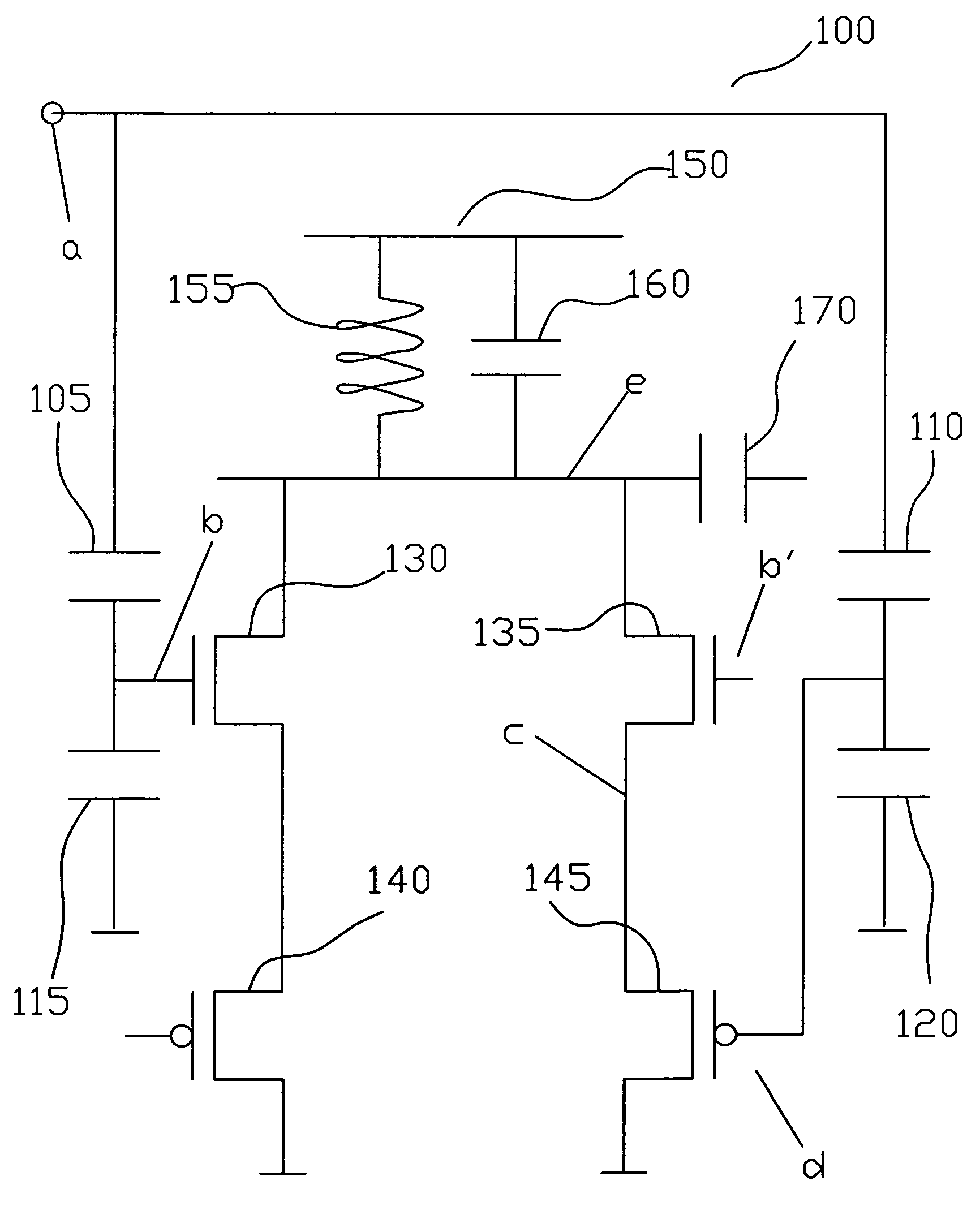
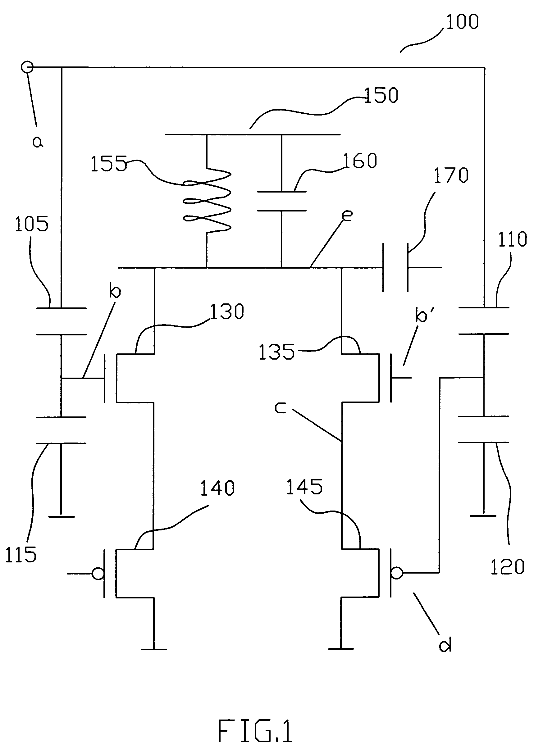
[0025]Refer to FIG. 1, which is a circuit schematic illustrating a CMOS single-ended frequency doubler according to an embodiment of the present invention.

[0026]As shown in FIG. 1, the CMOS single-ended frequency doubler 100 comprises a first capacitor 105 connected between a single-ended input node (a) and the gate of a first transistor 130. A second capacitor 115 is connected between the gate of the first transistor 130 and ground. The source of a first PMOS transistor 140 is connected to the source of the first transistor 130. The drain of the first PMOS transistor 140 is connected to ground.

[0027]A third capacitor 110 is connected between the single-ended input node (a) and the gate of a second P...


PUM


Abstract

A CMOS single-ended frequency doubler with improved subharmonic rejection and low phase noise which allows a single ended reference signal to be utilized in a Balanced Colpitts oscillator. The input is reproduced with a 180-degree phase shift for the opposite Colpitts transistor. This is achieved by adding two PMOS transistors. One transistor is placed as a follower, which reproduces any voltage shift applied to its gate to its source. Another transistor is a matching transistor for balance. By applying the single-ended signal to the gate of the follower transistor, it is reproduced at the source. The rest of the circuit takes advantage of the summing of two period currents with a 180-degree phase shift. The present invention achieves superior performance for frequency doubling due to the squaring of the gate voltage in the corresponding drain current. As a result, the double frequency component is further enhanced.

Description

BACKGROUND OF THE INVENTION[0001]1. Field of the Invention[0002]The present invention relates to an oscillator circuit. More specifically, the present invention discloses an efficient CMOS oscillator, which effectively doubles the frequency of a single-ended input signal.[0003]2. Description of the Prior Art[0004]The need for higher frequency reference signals has exacerbated the importance of frequency multiplication circuits that preserve phase noise at an affordable cost.[0005]While Phase Locked Loops (PLL) are widely used, a PLL's phase noise performance is mainly limited to that of its voltage control oscillator (VCO). For phase noise and jitter sensitive applications, non-PLL frequency multiplication is required, in particular frequency doublers.[0006]One type of frequency doubler uses a mixer to derive the higher frequency and filter out the subharmonics and undesired harmonics. However, these solutions only achieve limited harmonic and subharmonic rejection.[0007]Other disad...

Claims


Application Information

Patent Timeline
Patent Type & Authority Patents(United States)
IPC IPC(8): H03B5/12H03B5/34H03B9/14
CPCH03B19/14
Inventor GUEBELS, PIERRE PAUL
Owner MICROCHIP TECH INC
Learn More