Method of driving liquid crystal panel and apparatus

a liquid crystal display device and liquid crystal display technology, applied in the direction of instruments, static indicating devices, etc., can solve the problems of distortion image displayed on the liquid crystal panel, non-uniform light transmissivity, voltage at the right stage of scanning wiring, etc., to prevent image distortion

Inactive Publication Date: 2007-01-16
LG DISPLAY CO LTD
View PDF34 Cites 39 Cited by
  • Summary
  • Abstract
  • Description
  • Claims
  • Application Information

AI Technical Summary

Benefits of technology

[0010]Accordingly, it is an object of the present invention to provide a method of driving a liquid crystal panel which can prevent a distortion of an image as well as a non-uniform phenomenon in the light transmissivity due to the propagation delay in the scanning wiring, and an apparatus thereof.
[0011]Another object of the present invention is to provide a liquid crystal panel drive method and apparatus capable of securing an uniformity in the charging time of liquid crystal cells on a liquid crystal panel.

Problems solved by technology

This results in distortion of the voltage at the right stage of the scanning wiring 11 that is far away from the scanning voltage input terminal.
This results in the distortion image displayed on the liquid crystal panel being as well as a non-uniform light transmissivity in the liquid crystal panel.

Method used


Image

  • Method of driving liquid crystal panel and apparatus
  • Method of driving liquid crystal panel and apparatus
  • Method of driving liquid crystal panel and apparatus

Examples


first embodiment

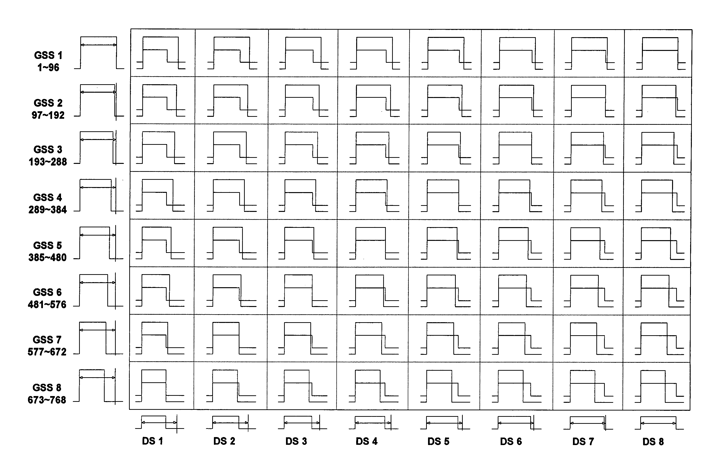
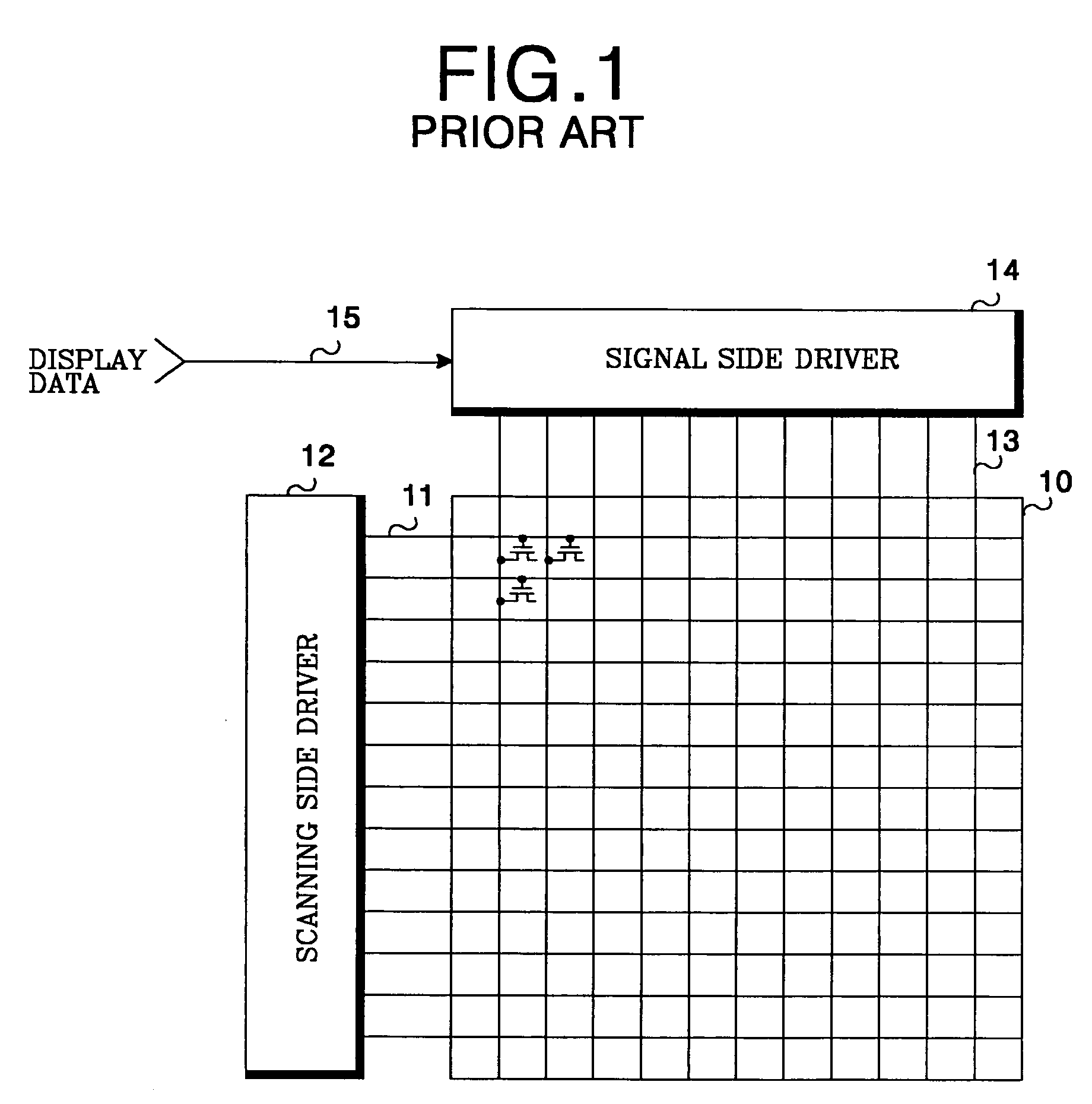
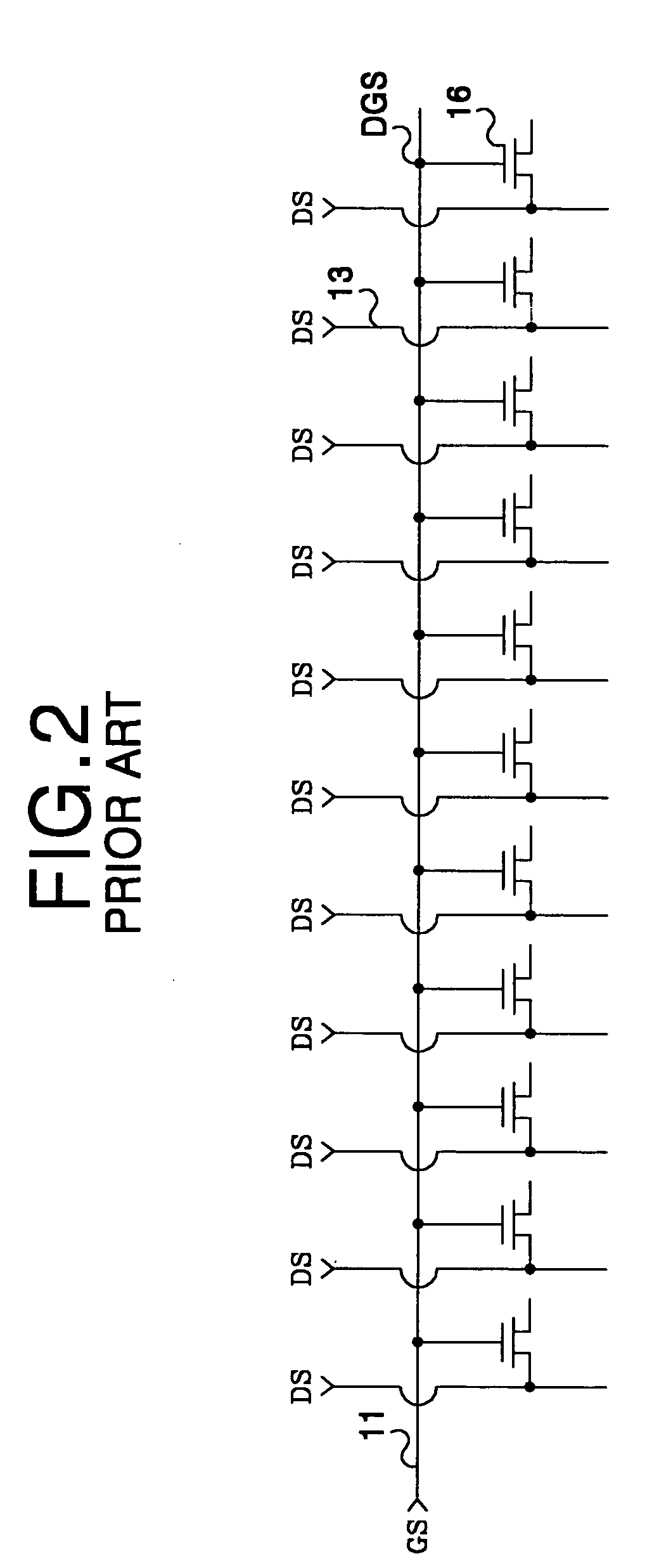
[0054]Referring to FIG. 8, there is shown a liquid crystal panel driving apparatus according to the present invention. As shown in FIG. 8, the liquid crystal panel driving apparatus includes gate driver IC (Integrated Circuit) chips 32A to 32E for driving a scanning wiring GL of a liquid crystal panel 30, and data driver IC chips 34A to 34H for driving a signal wiring DL of the liquid crystal panel 30. The scanning wiring GL includes a number of scanning lines, i.e., m scanning lines GL1 to GLm. Gate electrodes of a number of thin film transistors (not shown) are connected to each of the scanning lines GL1 to GLm. The gate driver IC chips 32A to 32E divisionally drives the scanning lines GL1 to GLm. Specifically, the gate driver IC chip 32A sequentially applies a gate signal to the 1st to (m / 5)th gate lines GL1 to GLm / 5 when a gate start pulse GSP is applied thereto through a gate carry line 31. Then, the 1st to (m / 5)th gate lines GL1 to GLm / 5 are sequentially driven with a scanning...

second embodiment

[0059]Referring now to FIG. 13, there is shown a liquid crystal panel driving apparatus according to the present invention. As shown in FIG. 13, the liquid crystal panel driving apparatus has a circuit configuration in which the first to seventh delay circuits 36A to 36G in FIG. 8 are replaced by a single of delay circuit 36 and an enable line 39 is commonly connected to first to seventh data driver IC chips 34A to 34G. The delay circuit 36 delays an output enable signal OE from the enable line 39 by a delay time of a scanning signal in a gate line GL and applies the delayed output enable signal to a eighth data driver IC chip 34H. Accordingly, the first to seventh data driver IC chips 34A to 34G apply k data signals to a liquid crystal panel 30 simultaneously, while the eighth data driver IC chip 34H applies k data signals to the liquid crystal panel 30 after a delay time in the gate line GL. According to this operation, a data signal is accurately applied to each of cells included...

third embodiment

[0060]Referring now to FIG. 14, there is shown a liquid crystal panel driving apparatus according to the present invention. As shown in FIG. 14, the liquid crystal panel driving apparatus includes gate driver IC chips 32A to 32E for driving a scanning wiring GL of a liquid crystal panel 30, and data driver IC chips 34A to 34H for driving a signal wiring DL of the liquid crystal panel 30. The scanning wiring GL includes a number of scanning lines, i.e., m scanning lines GL1 to GLm. Gate electrodes of a number of thin film transistors (not shown) are connected to each of the scanning lines GL1 to GLm. The gate driver IC chips 32A to 32E divisionally drives the scanning lines GL1 to GLm. Specifically, the gate driver IC chip 32A sequentially applies a gate signal to the 1st to (m / 5)th gate lines GL1 to GLm / 5 when a gate start pulse GSP is applied thereto through a gate carry line 31. Then, the 1st to (m / 5)th gate lines GL1 to GLm / 5 are sequentially driven with a scanning signal applied...


PUM

PropertyMeasurementUnit
voltageaaaaaaaaaa
voltageaaaaaaaaaa
voltage ΔVpaaaaaaaaaa

Abstract

A method and apparatus of driving a liquid crystal panel to prevent an image distortion and a non-uniform phenomenon in the light transmissivity caused by propagation delay in a scanning wiring of the liquid crystal panel. Data signal voltages are supplied to a signal wiring with a predetermined time interval in accordance with a delay characteristic of a scanning signal in the scanning wiring. Accordingly, even when the scanning signal is delayed in the scanning wiring, the data signal voltages are accurately applied to all liquid crystal cells and hence a picture displayed on the liquid crystal panel is not distorted.

Description

BACKGROUND OF THE INVENTION[0001]1. Field of the Invention[0002]This invention relates to a matrix type liquid crystal display device, and more particularly to a method of driving a liquid crystal panel including thin film transistors and an apparatus thereof.[0003]2. Description of the Prior Art[0004]Generally, in a matrix type liquid crystal display device with thin film transistors, the thin film transistors are provided in the liquid crystal display panel. This matrix type liquid crystal display device can produce a high contrast display even when driven at a low duty ratio or duty cycle in a multiple-line multiplex driving mode. As shown in FIG. 1, the matrix type liquid crystal display device consists of a liquid crystal panel 10 having a plurality of thin film transistors and a plurality of liquid crystal cells, and a scanning side driving circuit 12 and a signal side driving circuit 14 which are connected to the liquid crystal panel 10. The scanning side driving circuit 12 s...

Claims


Application Information

Patent Timeline
Patent Type & Authority Patents(United States)
IPC IPC(8): G09G3/36G02F1/133G09G3/20
CPCG09G3/3688G09G3/3677G09G2320/0223
Inventor JEONG, YUN CHEOLKIM, CHANG YEON
Owner LG DISPLAY CO LTD
Why Eureka
Try Eureka