

Inspection system for use with scanning electron microscope
An electron microscope and inspection system technology, applied in the field of inspection systems, can solve the problems of image difficulty, size limitation, pollution, etc. of the object to be inspected, and achieve the effect of correct inspection, cost realization, and inspection realization
- Summary
- Abstract
- Description
- Claims
- Application Information
AI Technical Summary
Problems solved by technology
Method used
Image

Examples
Embodiment Construction
[0034] The present invention will be described more fully hereinafter with reference to the accompanying drawings, in which exemplary embodiments of the invention are shown. As those skilled in the art would realize, the described embodiments may be modified in various different ways, all without departing from the spirit or scope of the present invention.
[0035] Descriptions of parts not related to the present invention are omitted, and like reference numerals designate like elements throughout the specification.
[0036] Therefore, will refer to Figure 1 to Figure 5 An inspection system using a scanning electron microscope according to an exemplary embodiment is described.
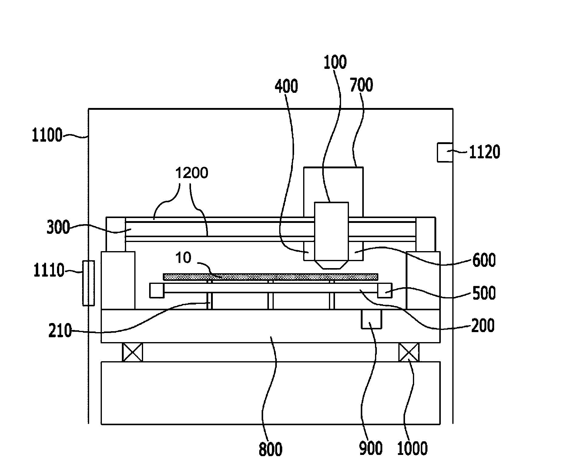
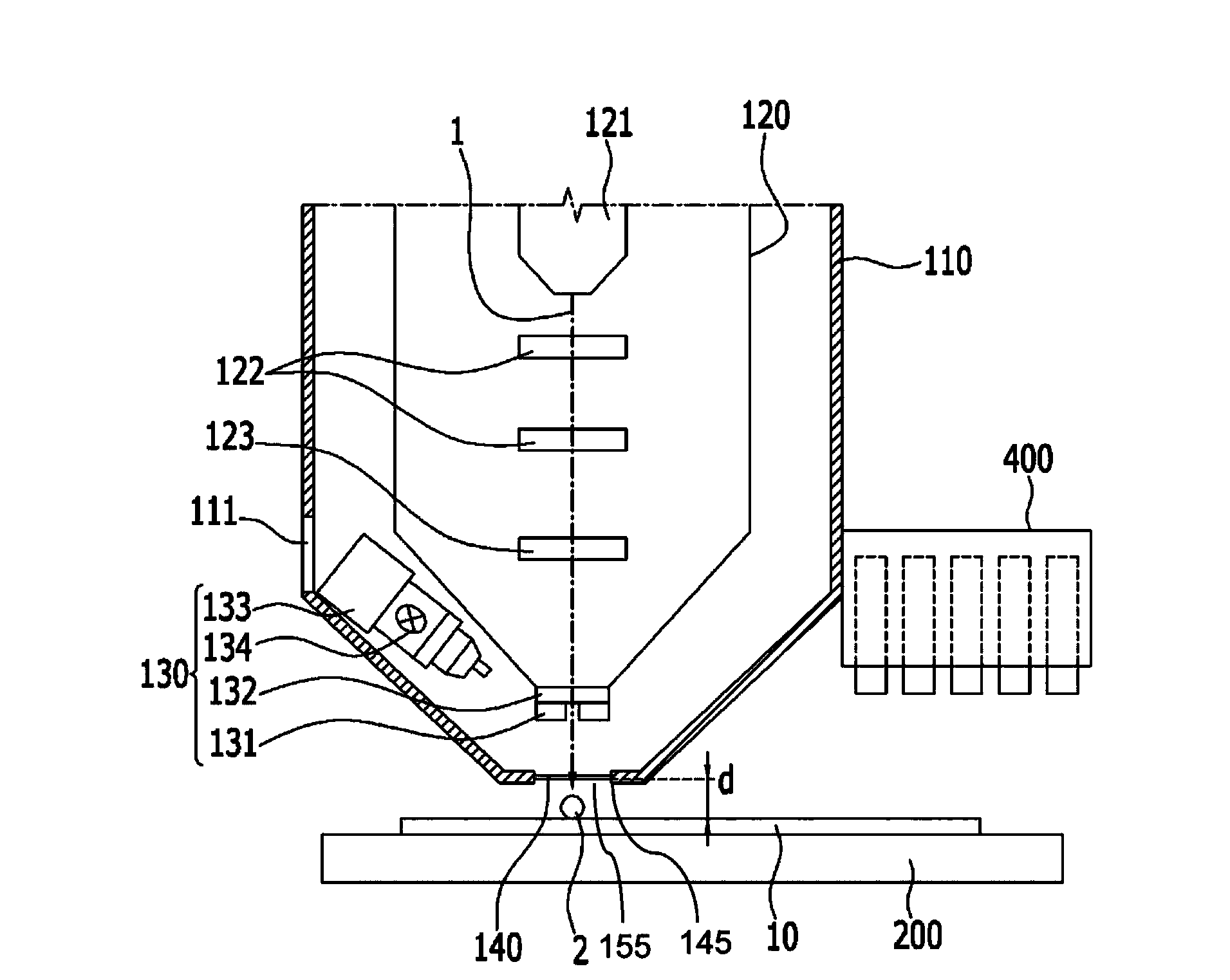
[0037] figure 1 is a schematic diagram of an inspection system using a scanning electron microscope according to an exemplary embodiment, figure 2 is an enlarged view of a scanning electron microscope chamber and a stage of an inspection system using a scanning electron microscope according to an ...
PUM
 Abstract
Description
Claims
Application Information