Hexagonal array structure of dielectric rod to shape flat-topped element pattern

a dielectric rod and array structure technology, applied in the direction of leaky waveguide antennas, electrical equipment, antennas, etc., can solve the problems of reducing efficiency, affecting the development of phased array antennas, and affecting the efficiency of the feed network, so as to achieve constant electric performance and wide beam scanning range

Inactive Publication Date: 2007-01-23
ELECTRONICS & TELECOMM RES INST
View PDF9 Cites 250 Cited by
  • Summary
  • Abstract
  • Description
  • Claims
  • Application Information

AI Technical Summary

Benefits of technology

[0014]It is, therefore, an object of the present invention to provide a hexagonal array structure of a dielectric rod for shaping a flat-topped element pattern (FTEP) for having a wide beam scanning range and a constant electric performance generated from a strong electromagnetic wave mutual coupling by arranging a dielectric rod at a vertex of a regular hexagon as a center dielectric rod and arranging a predetermined size of dielectric rods around the center dielectric rod.

Problems solved by technology

According to a Korea publication No. 10-2002-11503, entitled “Two dimensional multi layers circular radiation array structure for forming FTEP”, a phase control element is a major and expensive element for developing a phased array antenna.
However, according to the conventional array structures in FIGS. 1A to 1H, a feeding network is too complicated when it is implemented for the two-dimensional scanning.
Accordingly, the conventional array structures shown in FIGS. 1A to 1H have disadvantages such as decrease of efficiency, large volume, heavy weight and high system cost.
However, the conventional electric plane near scanning structure and the conventional magnetic plane linear scanning structure have comparative narrow bandwidth and a small beam scanning range.
Also, it is limited to be implemented in a one dimensional.
However, the wrinkled waveguide array structure requires a plurality of phase shifters since the space of the array elements is 0.7 to 0.85 λ and it is impossible designing more than 3% array antenna.
Also, the wrinkled waveguide array structure has disadvantages such as large volume, heavy weight and high system cost.

Method used


Image

  • Hexagonal array structure of dielectric rod to shape flat-topped element pattern
  • Hexagonal array structure of dielectric rod to shape flat-topped element pattern
  • Hexagonal array structure of dielectric rod to shape flat-topped element pattern

Examples


Embodiment Construction

[0027]Hereinafter, a hexagonal array structure of a dielectric rod for shaping a flat-topped element pattern (FTEP) in accordance with a preferred embodiment of the present invention will be described in more detail with reference to the accompanying drawings.

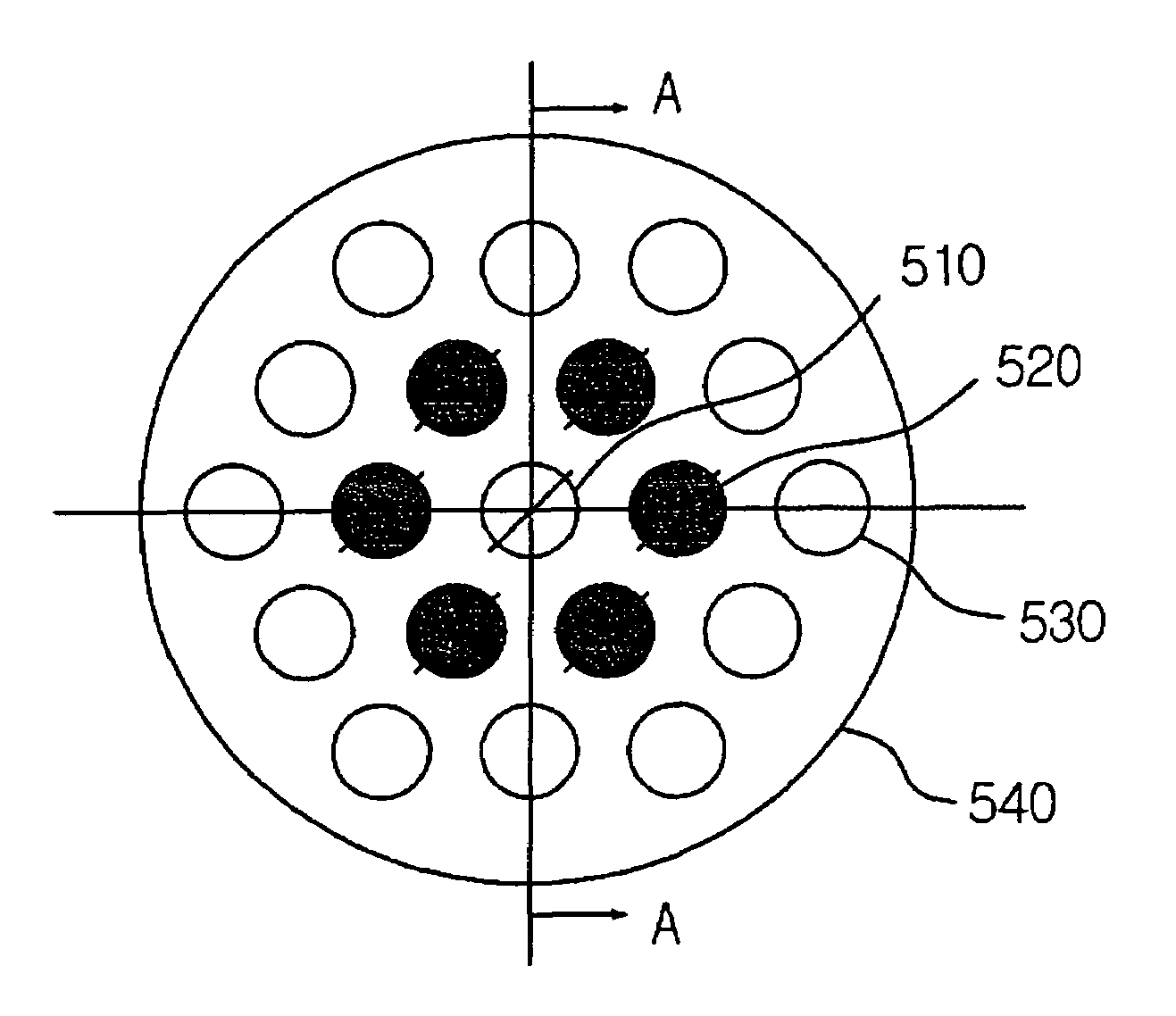
[0028]FIG. 5A is a side elevation view showing a hexagonal array structure of a dielectric rod for shaping a flat-topped element pattern (FTEP) in accordance with a preferred embodiment of the present invention. FIG. 5B is cross sectional view of a hexagonal array structure of a dielectric rod for shaping a flat-topped element pattern and FIG. 5C is an upper side elevation view of a hexagonal array structure of a dielectric rod in accordance with a preferred embodiment of the present invention.

[0029]The hexagonal array structure of a dielectric rod includes a center element 510, six of first ring elements 520, twelve of second ring elements 530 and a circular waveguide array supporting unit 540.

[0030]When a basic mode signal is...


PUM


Abstract

A hexagonal array structure of a dielectric rod for shaping a flat-topped element pattern (FTEP) is provided. The hexagonal structure of dielectric rods forming a flat-topped element pattern (FTEP) includes: a center element for forming a unit radiation pattern of the FTEP through an electromagnetic wave mutual coupling by receiving a polarization signal of a basic mode; a plurality of first ring elements arranged at vertexes of a regular hexagon based on the center element for forming the unit radiation pattern by electromagnetic wave mutual coupling with the center element and an electromagnetic wave; and a circular waveguide array supporting unit for supporting the center element and the plurality of first ring elements.

Description

FIELD OF THE INVENTION[0001]The present invention relates to a hexagonal array structure of a dielectric rod for shaping a flat-topped element pattern (FTEP); and, more particularly, to a hexagonal array structure of a dielectric rod for shaping a flat-topped element pattern (FTEP) for having a wide beam scanning range and a constant electric performance generated from a strong electromagnetic wave mutual coupling by arranging a dielectric rod at a vertex of a regular hexagon as a center dielectric rod and arranging a predetermined size of dielectric rods around the center dielectric rod.DESCRIPTION OF RELATED ARTS[0002]According to a Korea publication No. 10-2002-11503, entitled “Two dimensional multi layers circular radiation array structure for forming FTEP”, a phase control element is a major and expensive element for developing a phased array antenna. The number of the phase control elements is determined according to a gain of an antenna array, a side lobe level and a required...

Claims


Application Information

Patent Timeline
Patent Type & Authority Patents(United States)
IPC IPC(8): H01Q13/00H01Q13/24H01Q21/06
CPCH01Q21/067H01Q13/24H01Q21/06
Inventor KIM, YANG-SUKANG, BYUNG-SUKU, BON-JUNPARK, JONG-MINAHN, DO-SEOB
Owner ELECTRONICS & TELECOMM RES INST
Why Eureka
Try Eureka